- 您现在的位置:买卖IC网 > PDF目录10153 > LTC2140CUP-14#TRPBF (Linear Technology)IC ADC DUAL 14BIT 25 MSPS 64-QFN PDF资料下载
参数资料
| 型号: | LTC2140CUP-14#TRPBF |
| 厂商: | Linear Technology |
| 文件页数: | 15/38页 |
| 文件大小: | 0K |
| 描述: | IC ADC DUAL 14BIT 25 MSPS 64-QFN |
| 标准包装: | 2,000 |
| 位数: | 14 |
| 采样率(每秒): | 25M |
| 数据接口: | 并联,串行,SPI |
| 转换器数目: | 2 |
| 功率耗散(最大): | 202mW |
| 电压电源: | 模拟和数字 |
| 工作温度: | 0°C ~ 70°C |
| 安装类型: | 表面贴装 |
| 封装/外壳: | 64-WFQFN 裸露焊盘 |
| 供应商设备封装: | 64-QFN(9x9) |
| 包装: | 带卷 (TR) |
| 输入数目和类型: | 2 个差分 |
| 配用: | DC890B-ND - BOARD USB DATA COLLECTION |
第1页第2页第3页第4页第5页第6页第7页第8页第9页第10页第11页第12页第13页第14页当前第15页第16页第17页第18页第19页第20页第21页第22页第23页第24页第25页第26页第27页第28页第29页第30页第31页第32页第33页第34页第35页第36页第37页第38页
LTC2142-14/
LTC2141-14/LTC2140-14
22
21421014fa
APPLICATIONS INFORMATION
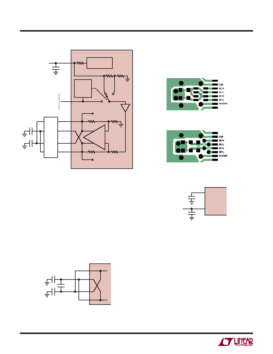
VREF
REFH
SENSE
C1
TIE TO VDD FOR 2V RANGE;
TIE TO GND FOR 1V RANGE;
SENSE FOR
0.625V < VSENSE < 1.300V
1.25V
REFL
INTERNAL ADC
HIGH REFERENCE
BUFFER
21421014 F08a
LTC2142
5Ω
0.8x
DIFF AMP
INTERNAL ADC
LOW REFERENCE
C1: 2.2μF LOW INDUCTANCE
INTERDIGITATED CAPACITOR
TDK CLLE1AX7S0G225M
MURATA LLA219C70G225M
AVX W2L14Z225M
OR EQUIVALENT
1.25V BANDGAP
REFERENCE
0.625V
RANGE
DETECT
AND
CONTROL
2.2μF
C2
0.1μF
C3
0.1μF
+
–
+
Figure 8a. Reference Circuit
SENSE
1.25V
EXTERNAL
REFERENCE
2.2μF
1μF
VREF
21421014 F09
LTC2142
Figure 9. Using an External 1.25V Reference
REFH
REFL
21421014 F08b
LTC2142
CAPACITORS ARE 0402 PACKAGE SIZE
C3
0.1μF
C1
2.2μF
C2
0.1μF
Figure 8b. Alternative REFH/REFL Bypass Circuit
Figure 8c. Recommended Layout for the REFH/REFL
Bypass Circuit in Figure 8a
Alternatively C1 can be replaced by a standard 2.2μF
capacitor between REFH and REFL (see Figure 8b). The
capacitors should be as close to the pins as possible (not
on the back side of the circuit board).
Figure 8c and Figure 8d show the recommended circuit
board layout for the REFH/REFL bypass capacitors. Note
that in Figure 8c, every pin of the interdigitated capacitor
(C1) is connected since the pins are not internally connected
in some vendors’ capacitors. In Figure 8d the REFH and
Figure 8d. Recommended Layout for the REFH/REFL
Bypass Circuit in Figure 8b
Encode Inputs
The signal quality of the encode inputs strongly affects
the A/D noise performance. The encode inputs should
be treated as analog signals – do not route them next to
digital traces on the circuit board. There are two modes
of operation for the encode inputs: the differential encode
mode (Figure 10), and the single-ended encode mode
(Figure 11).
The differential encode mode is recommended for si-
nusoidal, PECL, or LVDS encode inputs (Figure 12 and
Figure 13). The encode inputs are internally biased to 1.2V
through 10k equivalent resistance. The encode inputs can
be taken above VDD (up to 3.6V), and the common mode
range is from 1.1V to 1.6V. In the differential encode mode,
REFL pins are connected by short jumpers in an internal
layer. To minimize the inductance of these jumpers they
can be placed in a small hole in the GND plane on the
second board layer.
相关PDF资料 |
PDF描述 |
|---|---|
| LTC1605IG#TR | IC ADC 16BIT 5V SAMPLING 28SSOP |
| VE-22P-IW-F1 | CONVERTER MOD DC/DC 13.8V 100W |
| MS3100E28-11PX | CONN RCPT 22POS WALL MNT W/PINS |
| MS3100E28-11P | CONN RCPT 22POS WALL MNT W/PINS |
| SF4282-11EPG-3ES | CONN RCPT 11POS PNL MNT PIN |
相关代理商/技术参数 |
参数描述 |
|---|---|
| LTC2140IUP-12#PBF | 功能描述:IC ADC DUAL 12BIT 25MSPS 64-QFN RoHS:是 类别:集成电路 (IC) >> 数据采集 - 模数转换器 系列:- 标准包装:1,000 系列:- 位数:12 采样率(每秒):300k 数据接口:并联 转换器数目:1 功率耗散(最大):75mW 电压电源:单电源 工作温度:0°C ~ 70°C 安装类型:表面贴装 封装/外壳:24-SOIC(0.295",7.50mm 宽) 供应商设备封装:24-SOIC 包装:带卷 (TR) 输入数目和类型:1 个单端,单极;1 个单端,双极 |
| LTC2140IUP-12#TRPBF | 功能描述:IC ADC DUAL 12BIT 25MSPS 64-QFN RoHS:是 类别:集成电路 (IC) >> 数据采集 - 模数转换器 系列:- 标准包装:1,000 系列:- 位数:12 采样率(每秒):300k 数据接口:并联 转换器数目:1 功率耗散(最大):75mW 电压电源:单电源 工作温度:0°C ~ 70°C 安装类型:表面贴装 封装/外壳:24-SOIC(0.295",7.50mm 宽) 供应商设备封装:24-SOIC 包装:带卷 (TR) 输入数目和类型:1 个单端,单极;1 个单端,双极 |
| LTC2140IUP-14#PBF | 功能描述:IC ADC DUAL 14BIT 25 MSPS 64-QFN RoHS:是 类别:集成电路 (IC) >> 数据采集 - 模数转换器 系列:- 标准包装:1 系列:- 位数:14 采样率(每秒):83k 数据接口:串行,并联 转换器数目:1 功率耗散(最大):95mW 电压电源:双 ± 工作温度:0°C ~ 70°C 安装类型:通孔 封装/外壳:28-DIP(0.600",15.24mm) 供应商设备封装:28-PDIP 包装:管件 输入数目和类型:1 个单端,双极 |
| LTC2140IUP-14#TRPBF | 功能描述:IC ADC DUAL 14BIT 25 MSPS 64-QFN RoHS:是 类别:集成电路 (IC) >> 数据采集 - 模数转换器 系列:- 标准包装:1 系列:- 位数:14 采样率(每秒):83k 数据接口:串行,并联 转换器数目:1 功率耗散(最大):95mW 电压电源:双 ± 工作温度:0°C ~ 70°C 安装类型:通孔 封装/外壳:28-DIP(0.600",15.24mm) 供应商设备封装:28-PDIP 包装:管件 输入数目和类型:1 个单端,双极 |
| LTC2141-14 | 制造商:LINER 制造商全称:Linear Technology 功能描述:12-Bit, 65Msps/ 40Msps/25Msps Low Power Dual ADCs |
发布紧急采购,3分钟左右您将得到回复。