- 您现在的位置:买卖IC网 > PDF目录10153 > LTC2140CUP-14#TRPBF (Linear Technology)IC ADC DUAL 14BIT 25 MSPS 64-QFN PDF资料下载
参数资料
| 型号: | LTC2140CUP-14#TRPBF |
| 厂商: | Linear Technology |
| 文件页数: | 16/38页 |
| 文件大小: | 0K |
| 描述: | IC ADC DUAL 14BIT 25 MSPS 64-QFN |
| 标准包装: | 2,000 |
| 位数: | 14 |
| 采样率(每秒): | 25M |
| 数据接口: | 并联,串行,SPI |
| 转换器数目: | 2 |
| 功率耗散(最大): | 202mW |
| 电压电源: | 模拟和数字 |
| 工作温度: | 0°C ~ 70°C |
| 安装类型: | 表面贴装 |
| 封装/外壳: | 64-WFQFN 裸露焊盘 |
| 供应商设备封装: | 64-QFN(9x9) |
| 包装: | 带卷 (TR) |
| 输入数目和类型: | 2 个差分 |
| 配用: | DC890B-ND - BOARD USB DATA COLLECTION |
第1页第2页第3页第4页第5页第6页第7页第8页第9页第10页第11页第12页第13页第14页第15页当前第16页第17页第18页第19页第20页第21页第22页第23页第24页第25页第26页第27页第28页第29页第30页第31页第32页第33页第34页第35页第36页第37页第38页
23
21421014fa
LTC2142-14/
LTC2141-14/LTC2140-14
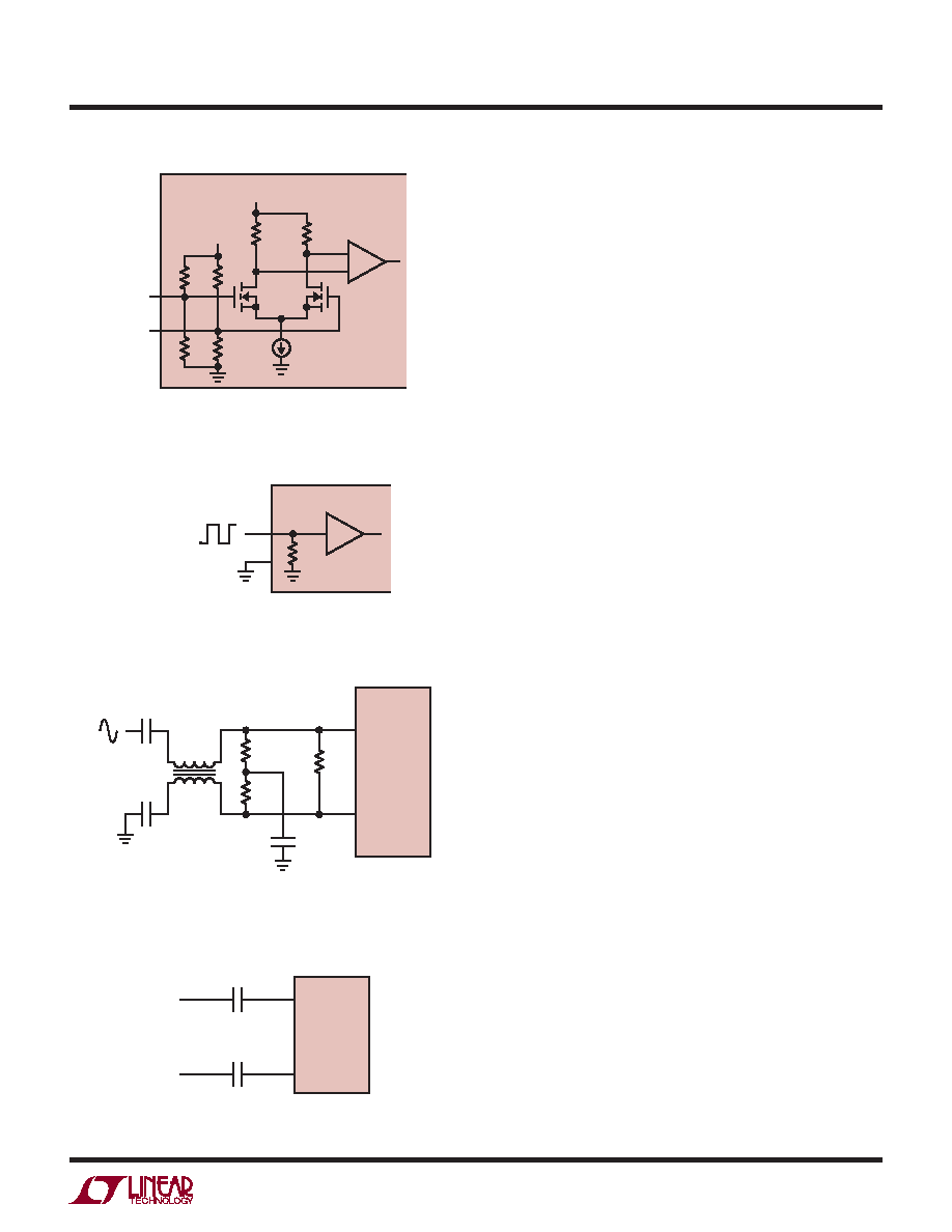
50Ω
100Ω
0.1μF
T1 = MA/COM ETC1-1-13
RESISTORS AND CAPACITORS
ARE 0402 PACKAGE SIZE
50Ω
LTC2142
21421014 F12
ENC–
ENC+
0.1μF
T1
Figure 12. Sinusoidal Encode Drive
ENC+
ENC–
PECL OR
LVDS
CLOCK
0.1μF
21421014 F13
LTC2142
Figure 13. PECL or LVDS Encode Drive
VDD
LTC2142
21421014 F10
ENC–
ENC+
15k
VDD
DIFFERENTIAL
COMPARATOR
30k
Figure 10. Equivalent Encode Input Circuit
for Differential Encode Mode
30k
ENC+
ENC–
21421014 F11
0V
1.8V TO 3.3V
LTC2142
CMOS LOGIC
BUFFER
Figure 11. Equivalent Encode Input Circuit
for Single-Ended Encode Mode
ENC– should stay at least 200mV above ground to avoid
falsely triggering the single ended encode mode. For good
jitter performance ENC+ and ENC– should have fast rise
and fall times.
The single-ended encode mode should be used with CMOS
encode inputs. To select this mode, ENC– is connected
to ground and ENC+ is driven with a square wave encode
input. ENC+ can be taken above VDD (up to 3.6V) so 1.8V
to 3.3V CMOS logic levels can be used. The ENC+ threshold
is 0.9V. For good jitter performance, ENC+ should have
fast rise and fall times.
If the encode signal is turned off or drops below approxi-
mately 500kHz, the A/D enters nap mode.
Clock Duty Cycle Stabilizer
For good performance the encode signal should have a
50% (±5%) duty cycle. If the optional clock duty cycle
stabilizer circuit is enabled, the encode duty cycle can
vary from 30% to 70% and the duty cycle stabilizer will
maintain a constant 50% internal duty cycle. If the encode
signal changes frequency, the duty cycle stabilizer circuit
requires one hundred clock cycles to lock onto the input
clock. The duty cycle stabilizer is enabled by mode control
register A2 (serial programming mode), or by CS (parallel
programming mode).
For applications where the sample rate needs to be changed
quickly, the clock duty cycle stabilizer can be disabled. If
the duty cycle stabilizer is disabled, care should be taken to
make the sampling clock have a 50% (±5%) duty cycle. The
duty cycle stabilizer should not be used below 5Msps.
DIGITAL OUTPUTS
Digital Output Modes
The LTC2142-14/LTC2141-14/LTC2140-14 can operate in
three digital output modes: full rate CMOS, double data
rate CMOS (to halve the number of output lines), or double
data rate LVDS (to reduce digital noise in the system.) The
output mode is set by mode control register A3 (serial
programming mode), or by SCK (parallel programming
mode). Note that double data rate CMOS cannot be selected
in the parallel programming mode.
APPLICATIONS INFORMATION
相关PDF资料 |
PDF描述 |
|---|---|
| LTC1605IG#TR | IC ADC 16BIT 5V SAMPLING 28SSOP |
| VE-22P-IW-F1 | CONVERTER MOD DC/DC 13.8V 100W |
| MS3100E28-11PX | CONN RCPT 22POS WALL MNT W/PINS |
| MS3100E28-11P | CONN RCPT 22POS WALL MNT W/PINS |
| SF4282-11EPG-3ES | CONN RCPT 11POS PNL MNT PIN |
相关代理商/技术参数 |
参数描述 |
|---|---|
| LTC2140IUP-12#PBF | 功能描述:IC ADC DUAL 12BIT 25MSPS 64-QFN RoHS:是 类别:集成电路 (IC) >> 数据采集 - 模数转换器 系列:- 标准包装:1,000 系列:- 位数:12 采样率(每秒):300k 数据接口:并联 转换器数目:1 功率耗散(最大):75mW 电压电源:单电源 工作温度:0°C ~ 70°C 安装类型:表面贴装 封装/外壳:24-SOIC(0.295",7.50mm 宽) 供应商设备封装:24-SOIC 包装:带卷 (TR) 输入数目和类型:1 个单端,单极;1 个单端,双极 |
| LTC2140IUP-12#TRPBF | 功能描述:IC ADC DUAL 12BIT 25MSPS 64-QFN RoHS:是 类别:集成电路 (IC) >> 数据采集 - 模数转换器 系列:- 标准包装:1,000 系列:- 位数:12 采样率(每秒):300k 数据接口:并联 转换器数目:1 功率耗散(最大):75mW 电压电源:单电源 工作温度:0°C ~ 70°C 安装类型:表面贴装 封装/外壳:24-SOIC(0.295",7.50mm 宽) 供应商设备封装:24-SOIC 包装:带卷 (TR) 输入数目和类型:1 个单端,单极;1 个单端,双极 |
| LTC2140IUP-14#PBF | 功能描述:IC ADC DUAL 14BIT 25 MSPS 64-QFN RoHS:是 类别:集成电路 (IC) >> 数据采集 - 模数转换器 系列:- 标准包装:1 系列:- 位数:14 采样率(每秒):83k 数据接口:串行,并联 转换器数目:1 功率耗散(最大):95mW 电压电源:双 ± 工作温度:0°C ~ 70°C 安装类型:通孔 封装/外壳:28-DIP(0.600",15.24mm) 供应商设备封装:28-PDIP 包装:管件 输入数目和类型:1 个单端,双极 |
| LTC2140IUP-14#TRPBF | 功能描述:IC ADC DUAL 14BIT 25 MSPS 64-QFN RoHS:是 类别:集成电路 (IC) >> 数据采集 - 模数转换器 系列:- 标准包装:1 系列:- 位数:14 采样率(每秒):83k 数据接口:串行,并联 转换器数目:1 功率耗散(最大):95mW 电压电源:双 ± 工作温度:0°C ~ 70°C 安装类型:通孔 封装/外壳:28-DIP(0.600",15.24mm) 供应商设备封装:28-PDIP 包装:管件 输入数目和类型:1 个单端,双极 |
| LTC2141-14 | 制造商:LINER 制造商全称:Linear Technology 功能描述:12-Bit, 65Msps/ 40Msps/25Msps Low Power Dual ADCs |
发布紧急采购,3分钟左右您将得到回复。