- 您现在的位置:买卖IC网 > PDF目录10043 > LTC2207IUK-14#TRPBF (Linear Technology)IC ADC 14BIT 105MSPS 48-QFN PDF资料下载
参数资料
| 型号: | LTC2207IUK-14#TRPBF |
| 厂商: | Linear Technology |
| 文件页数: | 17/32页 |
| 文件大小: | 0K |
| 描述: | IC ADC 14BIT 105MSPS 48-QFN |
| 标准包装: | 2,000 |
| 位数: | 14 |
| 采样率(每秒): | 105M |
| 数据接口: | 并联 |
| 转换器数目: | 1 |
| 功率耗散(最大): | 1.07W |
| 电压电源: | 单电源 |
| 工作温度: | -40°C ~ 85°C |
| 安装类型: | 表面贴装 |
| 封装/外壳: | 48-WFQFN 裸露焊盘 |
| 供应商设备封装: | 48-QFN-EP(7x7) |
| 包装: | 带卷 (TR) |
| 输入数目和类型: | 1 个差分 |
| 配用: | DC890B-ND - BOARD USB DATA COLLECTION |
第1页第2页第3页第4页第5页第6页第7页第8页第9页第10页第11页第12页第13页第14页第15页第16页当前第17页第18页第19页第20页第21页第22页第23页第24页第25页第26页第27页第28页第29页第30页第31页第32页
LTC2207-14/LTC2206-14
24
220714614fc
APPLICATIONS INFORMATION
converter data to the digital system. This is necessary
when using a sinusoidal encode. Data can be latched on the
rising edge of CLKOUT+ or the falling edge of CLKOUT–.
CLKOUT+ falls and CLKOUT– rises as the data outputs
are updated.
Digital Output Randomizer
Interference from the ADC digital outputs is sometimes
unavoidable. Interference from the digital outputs may be
from capacitive or inductive coupling or coupling through
the ground plane. Even a tiny coupling factor can result in
discernible unwanted tones in the ADC output spectrum.
By randomizing the digital output before it is transmitted
off chip, these unwanted tones can be randomized, trading
a slight increase in the noise oor for a large reduction in
unwanted tone amplitude.
The digital output is “Randomized” by applying an exclu-
sive-OR logic operation between the LSB and all other data
output bits. To decode, the reverse operation is applied;
that is, an exclusive-OR operation is applied between the
LSB and all other bits. The LSB, OF and CLKOUT outputs
are not affected. The output Randomizer function is active
when the RAND pin is high.
Output Driver Power
Separate output power and ground pins allow the output
drivers to be isolated from the analog circuitry. The power
supply for the digital output buffers, OVDD, should be tied
to the same power supply as for the logic being driven.
For example, if the converter is driving a DSP powered
by a 1.8V supply, then OVDD should be tied to that same
1.8V supply. In CMOS mode OVDD can be powered with
any logic voltage up to the VDD of the ADC. OGND can be
powered with any voltage from ground up to 1V and must
be less than OVDD. The logic outputs will swing between
OGND and OVDD.
Internal Dither
The LTC2207-14/LTC2206-14 are 14-bit ADCs with a very
linear transfer function; however, at low input levels even
slight imperfections in the transfer function will result in
unwanted tones. Small errors in the transfer function are
usually a result of ADC element mismatches. An optional
internal dither mode can be enabled to randomize the input
location on the ADC transfer curve, resulting in improved
SFDR for low signal levels.
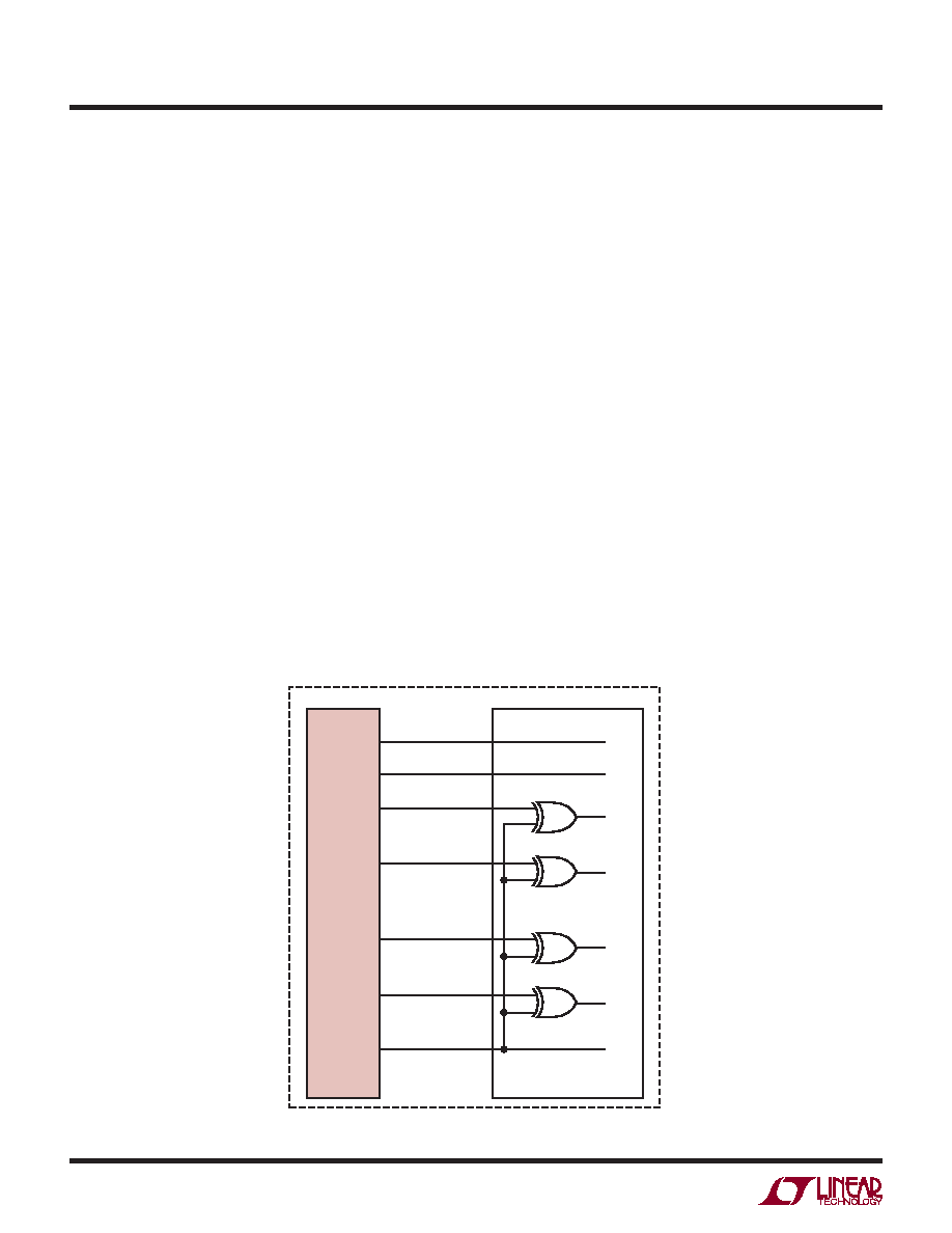
Figure 13. Descrambling a Scrambled Digital Output
D1
D0
D2
D12
D13
LTC2207-14/
LTC2206-14
PC BOARD
FPGA
CLKOUT
OF
D13/D0
D12/D0
D2/D0
D1/D0
D0
2207614 F13
相关PDF资料 |
PDF描述 |
|---|---|
| MS3108E20-11P | CONN PLUG 13POS RT ANG W/PINS |
| IDT72811L15TF | IC FIFO SYNC DUAL 512X9 64QFP |
| VI-2VX-MY | CONVERTER MOD DC/DC 5.2V 50W |
| LT1134AIN#PBF | IC 4DRV/4RCV RS232 5V 24-DIP |
| AD774BKN | IC ADC 12BIT W/BUFF REF 28-DIP |
相关代理商/技术参数 |
参数描述 |
|---|---|
| LTC2207UK | 制造商:LINER 制造商全称:Linear Technology 功能描述:16-Bit, 105Msps/80Msps ADCs |
| LTC2207UK-14 | 制造商:LINER 制造商全称:Linear Technology 功能描述:14-Bit, 105Msps/80Msps ADCs |
| LTC2208 | 制造商:LINER 制造商全称:Linear Technology 功能描述:Dual 14-Bit 250Msps |
| LTC2208-14 | 制造商:LINER 制造商全称:Linear Technology 功能描述:14-Bit, 130Msps ADC |
| LTC2208CUP | 制造商:Linear Technology 功能描述:IC ADC 16BIT 130MSPS 64-QFN |
发布紧急采购,3分钟左右您将得到回复。