- 您现在的位置:买卖IC网 > PDF目录10043 > LTC2207IUK-14#TRPBF (Linear Technology)IC ADC 14BIT 105MSPS 48-QFN PDF资料下载
参数资料
| 型号: | LTC2207IUK-14#TRPBF |
| 厂商: | Linear Technology |
| 文件页数: | 7/32页 |
| 文件大小: | 0K |
| 描述: | IC ADC 14BIT 105MSPS 48-QFN |
| 标准包装: | 2,000 |
| 位数: | 14 |
| 采样率(每秒): | 105M |
| 数据接口: | 并联 |
| 转换器数目: | 1 |
| 功率耗散(最大): | 1.07W |
| 电压电源: | 单电源 |
| 工作温度: | -40°C ~ 85°C |
| 安装类型: | 表面贴装 |
| 封装/外壳: | 48-WFQFN 裸露焊盘 |
| 供应商设备封装: | 48-QFN-EP(7x7) |
| 包装: | 带卷 (TR) |
| 输入数目和类型: | 1 个差分 |
| 配用: | DC890B-ND - BOARD USB DATA COLLECTION |
第1页第2页第3页第4页第5页第6页当前第7页第8页第9页第10页第11页第12页第13页第14页第15页第16页第17页第18页第19页第20页第21页第22页第23页第24页第25页第26页第27页第28页第29页第30页第31页第32页
LTC2207-14/LTC2206-14
15
220714614fc
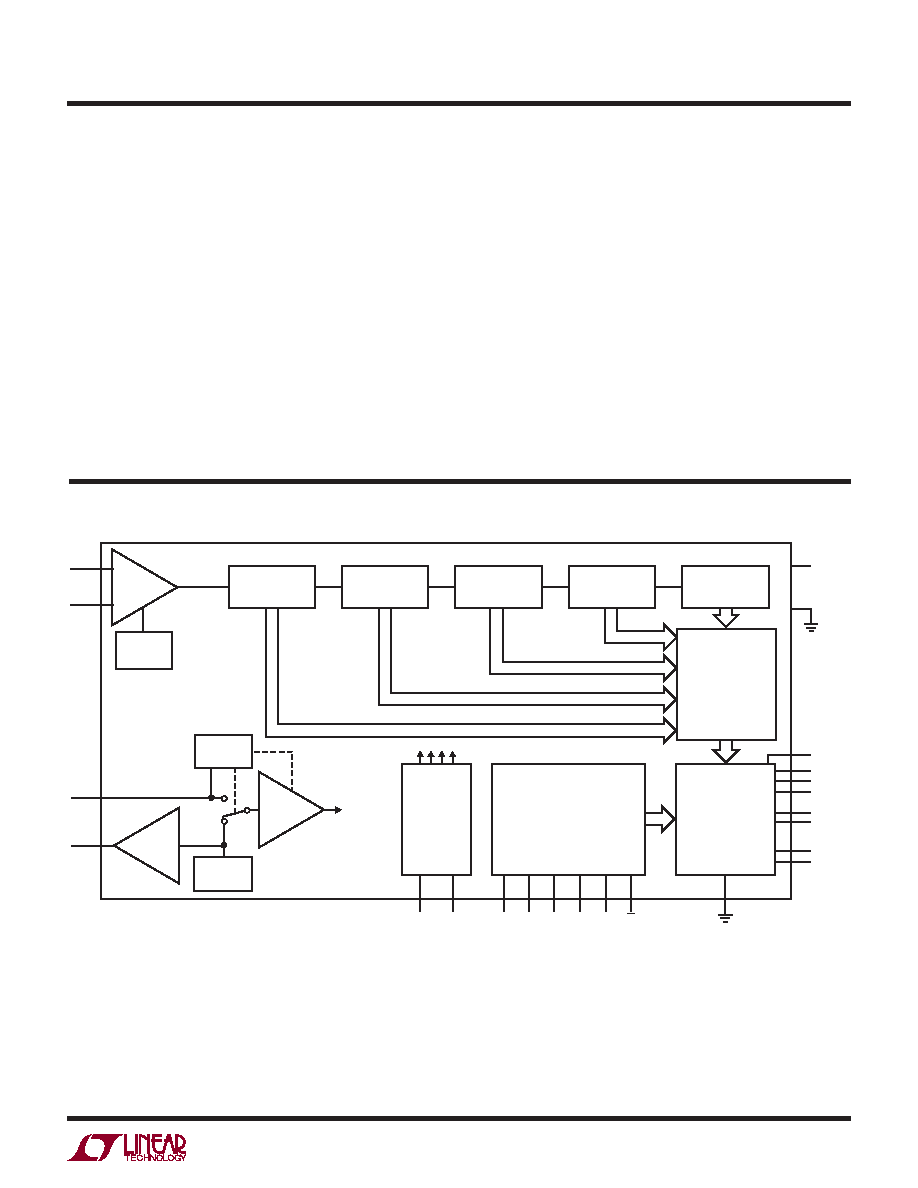
PIN FUNCTIONS
OF (Pin 43): Over/Under Flow Digital Output. OF is high
when an over or under ow has occurred.
OE (Pin 44): Output Enable Pin. Low enables the digital
output drivers. High puts digital outputs in Hi-Z state.
MODE (Pin 45): Output Format and Clock Duty Cycle
Stabilizer Selection Pin. Connecting MODE to 0V selects
offset binary output format and disables the clock duty
cycle stabilizer. Connecting MODE to 1/3VDD selects offset
binary output format and enables the clock duty cycle sta-
bilizer. Connecting MODE to 2/3VDDselects2’scomplement
output format and enables the clock duty cycle stabilizer.
Connecting MODE to VDD selects 2’s complement output
format and disables the clock duty cycle stabilizer.
RAND (Pin 46): Digital Output Randomization Selection
Pin. RAND low results in normal operation. RAND high
selects D1-D13 to be EXCLUSIVE-ORed with D0 (the
LSB). The output can be decoded by again applying an
XOR operation between the LSB and all other bits. This
mode of operation reduces the effects of digital output
interference.
PGA(Pin47):ProgrammableGainAmplierControlPin.Low
selects a front-end gain of 1, input range of 2.25VP-P. High
selects a front-end gain of 1.5, input range of 1.5VP-P.
GND (Exposed Pad, Pin 49): ADC Power Ground. The ex-
posed pad on the bottom of the package must be soldered
to ground.
DITH
OE
MODE
PGA RAND
SHDN
ADC CLOCKS
DIFFERENTIAL
INPUT
LOW JITTER
CLOCK
DRIVER
DITHER
SIGNAL
GENERATOR
FIRST PIPELINED
ADC STAGE
FIFTH PIPELINED
ADC STAGE
FOURTH PIPELINED
ADC STAGE
SECOND PIPELINED
ADC STAGE
ENC+
ENC–
CORRECTION LOGIC
AND
SHIFT REGISTER
OGND
CLKOUT+
CLKOUT–
OF
D13
D12
OVDD
D1
D0
2207614 F01
INPUT
S/H
AIN
–
AIN
+
THIRD PIPELINED
ADC STAGE
OUTPUT
DRIVERS
CONTROL
LOGIC
VDD
GND
PGA
SENSE
VCM
BUFFER
ADC
REFERENCE
VOLTAGE
REFERENCE
RANGE
SELECT
Figure 1. Functional Block Diagram
BLOCK DIAGRAM
相关PDF资料 |
PDF描述 |
|---|---|
| MS3108E20-11P | CONN PLUG 13POS RT ANG W/PINS |
| IDT72811L15TF | IC FIFO SYNC DUAL 512X9 64QFP |
| VI-2VX-MY | CONVERTER MOD DC/DC 5.2V 50W |
| LT1134AIN#PBF | IC 4DRV/4RCV RS232 5V 24-DIP |
| AD774BKN | IC ADC 12BIT W/BUFF REF 28-DIP |
相关代理商/技术参数 |
参数描述 |
|---|---|
| LTC2207UK | 制造商:LINER 制造商全称:Linear Technology 功能描述:16-Bit, 105Msps/80Msps ADCs |
| LTC2207UK-14 | 制造商:LINER 制造商全称:Linear Technology 功能描述:14-Bit, 105Msps/80Msps ADCs |
| LTC2208 | 制造商:LINER 制造商全称:Linear Technology 功能描述:Dual 14-Bit 250Msps |
| LTC2208-14 | 制造商:LINER 制造商全称:Linear Technology 功能描述:14-Bit, 130Msps ADC |
| LTC2208CUP | 制造商:Linear Technology 功能描述:IC ADC 16BIT 130MSPS 64-QFN |
发布紧急采购,3分钟左右您将得到回复。