- 您现在的位置:买卖IC网 > PDF目录10043 > LTC2207IUK-14#TRPBF (Linear Technology)IC ADC 14BIT 105MSPS 48-QFN PDF资料下载
参数资料
| 型号: | LTC2207IUK-14#TRPBF |
| 厂商: | Linear Technology |
| 文件页数: | 6/32页 |
| 文件大小: | 0K |
| 描述: | IC ADC 14BIT 105MSPS 48-QFN |
| 标准包装: | 2,000 |
| 位数: | 14 |
| 采样率(每秒): | 105M |
| 数据接口: | 并联 |
| 转换器数目: | 1 |
| 功率耗散(最大): | 1.07W |
| 电压电源: | 单电源 |
| 工作温度: | -40°C ~ 85°C |
| 安装类型: | 表面贴装 |
| 封装/外壳: | 48-WFQFN 裸露焊盘 |
| 供应商设备封装: | 48-QFN-EP(7x7) |
| 包装: | 带卷 (TR) |
| 输入数目和类型: | 1 个差分 |
| 配用: | DC890B-ND - BOARD USB DATA COLLECTION |
第1页第2页第3页第4页第5页当前第6页第7页第8页第9页第10页第11页第12页第13页第14页第15页第16页第17页第18页第19页第20页第21页第22页第23页第24页第25页第26页第27页第28页第29页第30页第31页第32页
LTC2207-14/LTC2206-14
14
220714614fc
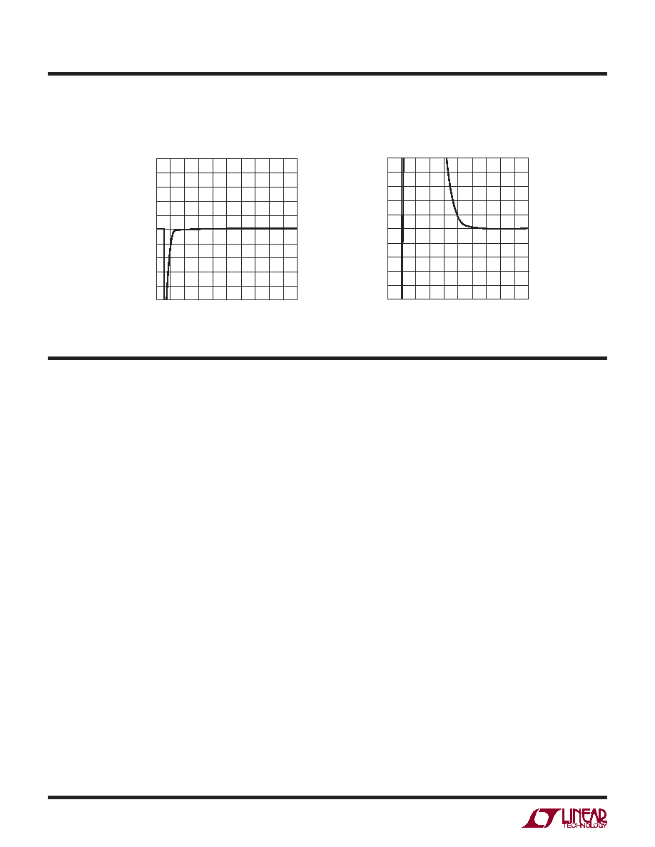
TYPICAL PERFORMANCE CHARACTERISTICS
TIME AFTER WAKE-UP OR CLOCK START (μs)
0
FULL-SCALE
ERROR
(%)
0.2
0.6
1.0
400
2207614 G60
–0.2
–0.6
0
0.4
0.8
–0.4
–0.8
–1.0
100
50
200
150
300 350
450
250
500
TIME FROM WAKE-UP OR CLOCK START (μs)
0
FULL-SCALE
ERROR
(%)
1
3
5
800
2207614 G61
–1
–3
0
2
4
–2
–4
–5
200
100
400
300
600 700
900
500
1000
Mid-Scale Settling After Wake
Up from Shutdown or Starting
Encode Clock
Full-Scale Settling After Wake
Up from Shutdown or Starting
Encode Clock
SENSE (Pin 1): Reference Mode Select and External
Reference Input. Tie SENSE to VDD to select the internal
2.5V bandgap reference. An external reference of 2.5V or
1.25V may be used; both reference values will set a full
scale ADC range of 2.25V (PGA = 0).
VCM(Pin2):1.25VOutput.Optimumvoltageforinputcom-
mon mode. Must be bypassed to ground with a minimum
of 2.2μF. Ceramic chip capacitors are recommended.
VDD (Pins 3, 4, 12, 13, 14): 3.3V Analog Supply Pin.
Bypass to GND with 0.1μF ceramic chip capacitors.
GND (Pins 5, 8, 11, 15, 48): ADC Power Ground.
AIN+ (Pin 6): Positive Differential Analog Input.
AIN– (Pin 7): Negative Differential Analog Input.
ENC+ (Pin 9): Positive Differential Encode Input. The
sampled analog input is held on the rising edge of ENC+.
Internally biased to 1.6V through a 6.2k resistor. Output
data can be latched on the rising edge of ENC+.
ENC– (Pin 10): Negative Differential Encode Input. The
sampled analog input is held on the falling edge of ENC–.
Internally biased to 1.6V through a 6.2k resistor. Bypass to
ground with a 0.1μF capacitor for a single-ended Encode
signal.
SHDN (Pin 16): Power Shutdown Pin. SHDN = low results
in normal operation. SHDN = high results in powered
down analog circuitry and the digital outputs are placed
in a high impedance state.
DITH (Pin 17): Internal Dither Enable Pin. DITH = low
disables internal dither. DITH = high enables internal dither.
Refer to Internal Dither section of this data sheet for details
on dither operation.
NC (Pins 18, 19): No Connect.
D0-D13 (Pins 20-22, 26-28, 32-35 and 39-42): Digital
Outputs. D13 is the MSB.
OGND (Pins 23, 31 and 38): Output Driver Ground.
OVDD (Pins 24, 25, 36, 37): Positive Supply for the Output
Drivers. Bypass to ground with 0.1μF capacitor.
CLKOUT– (Pin 29): Data Valid Output. CLKOUT– will toggle
at the sample rate. Latch the data on the falling edge of
CLKOUT–.
CLKOUT+ (Pin 30): Inverted Data Valid Output. CLKOUT+
will toggle at the sample rate. Latch the data on the rising
edge of CLKOUT+.
PIN FUNCTIONS
相关PDF资料 |
PDF描述 |
|---|---|
| MS3108E20-11P | CONN PLUG 13POS RT ANG W/PINS |
| IDT72811L15TF | IC FIFO SYNC DUAL 512X9 64QFP |
| VI-2VX-MY | CONVERTER MOD DC/DC 5.2V 50W |
| LT1134AIN#PBF | IC 4DRV/4RCV RS232 5V 24-DIP |
| AD774BKN | IC ADC 12BIT W/BUFF REF 28-DIP |
相关代理商/技术参数 |
参数描述 |
|---|---|
| LTC2207UK | 制造商:LINER 制造商全称:Linear Technology 功能描述:16-Bit, 105Msps/80Msps ADCs |
| LTC2207UK-14 | 制造商:LINER 制造商全称:Linear Technology 功能描述:14-Bit, 105Msps/80Msps ADCs |
| LTC2208 | 制造商:LINER 制造商全称:Linear Technology 功能描述:Dual 14-Bit 250Msps |
| LTC2208-14 | 制造商:LINER 制造商全称:Linear Technology 功能描述:14-Bit, 130Msps ADC |
| LTC2208CUP | 制造商:Linear Technology 功能描述:IC ADC 16BIT 130MSPS 64-QFN |
发布紧急采购,3分钟左右您将得到回复。