- 您现在的位置:买卖IC网 > PDF目录2005 > LTC2224IUK#TRPBF (Linear Technology)IC ADC 12BIT 135MSPS SAMPL 48QFN PDF资料下载
参数资料
| 型号: | LTC2224IUK#TRPBF |
| 厂商: | Linear Technology |
| 文件页数: | 10/24页 |
| 文件大小: | 0K |
| 描述: | IC ADC 12BIT 135MSPS SAMPL 48QFN |
| 标准包装: | 2,000 |
| 位数: | 12 |
| 采样率(每秒): | 135M |
| 数据接口: | 并联 |
| 转换器数目: | 1 |
| 功率耗散(最大): | 680mW |
| 电压电源: | 单电源 |
| 工作温度: | -40°C ~ 85°C |
| 安装类型: | 表面贴装 |
| 封装/外壳: | 48-WFQFN 裸露焊盘 |
| 供应商设备封装: | 48-QFN-EP(7x7) |
| 包装: | 带卷 (TR) |
| 输入数目和类型: | 1 个单端,双极; 1 个差分,双极 |
LTC2224
18
2224fa
APPLICATIO S I FOR ATIO
WU
UU
DIGITAL OUTPUTS
Table 1 shows the relationship between the analog input
voltage, the digital data bits and the overflow bit.
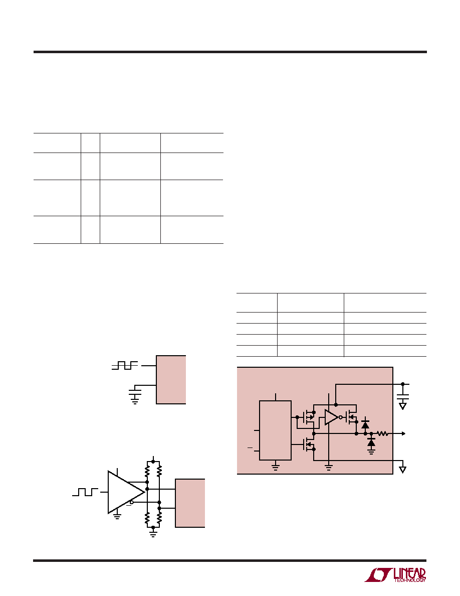
Digital Output Buffers
Figure 13 shows an equivalent circuit for a single output
buffer. Each buffer is powered by OVDD and OGND, which
are isolated from the ADC power and ground. The addi-
tional N-channel transistor in the output driver allows
operation down to voltages as low as 0.5V. The internal
resistor in series with the output makes the output appear
as 50
to external circuitry and may eliminate the need for
external damping resistors.
2224 F12a
ENC–
1.6V
VTHRESHOLD = 1.6V
ENC+
0.1
F
LTC2224
2224 F12b
ENC–
ENC+
130
3.3V
130
D0
Q0
MC100LVELT22
LTC2224
83
83
Figure 12a. Single-Ended ENC Drive,
Not Recommended for Low Jitter
Figure 12b. ENC Drive Using a CMOS to PECL Translator
As with all high speed/high resolution converters, the
digital output loading can affect the performance. The
digital outputs of the LTC2224 should drive a minimal
capacitive load to avoid possible interaction between the
digital outputs and sensitive input circuitry. For full speed
operation the capacitive load should be kept under 5pF.
Lower OVDD voltages will also help reduce interference
from the digital outputs and improve the SNR.
Data Format
The LTC2224 parallel digital output can be selected for
offset binary or 2’s complement format. The format is
selected with the MODE pin. Connecting MODE to GND or
1/3VDD selects offset binary output format. Connecting
MODE to 2/3VDD or VDD selects 2’s complement output
format. An external resistor divider can be used to set the
1/3VDD or 2/3VDD logic values. Table 2 shows the logic
states for the MODE pin.
LTC2224
2224 F13
OVDD
VDD
0.1
F
43
TYPICAL
DATA
OUTPUT
OGND
OVDD
0.5V
TO 3.6V
PREDRIVER
LOGIC
DATA
FROM
LATCH
OE
Figure 13. Digital Output Buffer
Table 1. Output Codes vs Input Voltage
AIN
+ – AIN–
D11 – D0
(2V Range)
OF
(Offset Binary)
(2’s Complement)
>+1.000000V
1
1111 1111 1111
0111 1111 1111
+0.999512V
0
1111 1111 1111
0111 1111 1111
+0.999024V
0
1111 1111 1110
0111 1111 1110
+0.000488V
0
1000 0000 0001
0000 0000 0001
0.000000V
0
1000 0000 0000
0000 0000 0000
–0.000488V
0
0111 1111 1111
1111 1111 1111
–0.000976V
0
0111 1111 1110
1111 1111 1110
–0.999512V
0
0000 0000 0001
1000 0000 0001
–1.000000V
0
0000 0000 0000
1000 0000 0000
<–1.000000V
1
0000 0000 0000
1000 0000 0000
Table 2. MODE Pin Function
Clock Duty
MODE Pin
Output Format
Cycle Stablizer
0
Offset Binary
Off
1/3VDD
Offset Binary
On
2/3VDD
2’s Complement
On
VDD
2’s Complement
Off
相关PDF资料 |
PDF描述 |
|---|---|
| LTC2225IUH#TRPBF | IC ADC 12BIT 10MSPS 3V 32-QFN |
| LTC2228IUH#TRPBF | IC ADC 12BIT 65MSPS SAMPL 32-QFN |
| LTC2229IUH#PBF | IC ADC 12-BIT 80MSPS 3V 32-QFN |
| LTC2231IUP#TRPBF | IC ADC 10BIT 135MSPS 64-QFN |
| LTC2233CUK#TRPBF | IC ADC 10BIT 80MSPS SAMPL 48QFN |
相关代理商/技术参数 |
参数描述 |
|---|---|
| LTC2224UK | 制造商:LINER 制造商全称:Linear Technology 功能描述:12-Bit, 135Msps ADC |
| LTC2225 | 制造商:LINER 制造商全称:Linear Technology 功能描述:14-Bit, 80Msps Low Power 3V ADC |
| LTC2225CUH | 制造商:Linear Technology 功能描述:ADC Single Pipelined 10Msps 12-bit Parallel 32-Pin QFN EP |
| LTC2225CUH#PBF | 功能描述:IC ADC 12-BIT 10MSPS 3V 32-QFN RoHS:是 类别:集成电路 (IC) >> 数据采集 - 模数转换器 系列:- 标准包装:1 系列:microPOWER™ 位数:8 采样率(每秒):1M 数据接口:串行,SPI? 转换器数目:1 功率耗散(最大):- 电压电源:模拟和数字 工作温度:-40°C ~ 125°C 安装类型:表面贴装 封装/外壳:24-VFQFN 裸露焊盘 供应商设备封装:24-VQFN 裸露焊盘(4x4) 包装:Digi-Reel® 输入数目和类型:8 个单端,单极 产品目录页面:892 (CN2011-ZH PDF) 其它名称:296-25851-6 |
| LTC2225CUH#TR | 制造商:Linear Technology 功能描述:ADC Single Pipelined 10Msps 12-bit Parallel 32-Pin QFN EP T/R |
发布紧急采购,3分钟左右您将得到回复。