参数资料
| 型号: | LTC2240CUP-12#PBF |
| 厂商: | Linear Technology |
| 文件页数: | 7/30页 |
| 文件大小: | 0K |
| 描述: | IC ADC 12BIT 170MSPS 64-QFN |
| 标准包装: | 40 |
| 位数: | 12 |
| 采样率(每秒): | 170M |
| 数据接口: | 并联 |
| 转换器数目: | 1 |
| 功率耗散(最大): | 638mW |
| 电压电源: | 单电源 |
| 工作温度: | 0°C ~ 70°C |
| 安装类型: | 表面贴装 |
| 封装/外壳: | 64-WFQFN 裸露焊盘 |
| 供应商设备封装: | 64-QFN(9x9) |
| 包装: | 管件 |
| 输入数目和类型: | 1 个差分,双极 |
第1页第2页第3页第4页第5页第6页当前第7页第8页第9页第10页第11页第12页第13页第14页第15页第16页第17页第18页第19页第20页第21页第22页第23页第24页第25页第26页第27页第28页第29页第30页
LTC2240-12
15
224012fd
APPLICATIONS INFORMATION
Each pipelined stage shown in Figure 1 contains an ADC,
a reconstruction DAC and an interstage residue amplier.
In operation, the ADC quantizes the input to the stage and
the quantized value is subtracted from the input by the
DAC to produce a residue. The residue is amplied and
output by the residue amplier. Successive stages operate
out of phase so that when the odd stages are outputting
their residue, the even stages are acquiring that residue
and vice versa.
When ENC is low, the analog input is sampled differentially
directly onto the input sample-and-hold capacitors, inside
the “Input S/H” shown in the block diagram. At the instant
that ENC transitions from low to high, the sampled input is
held. While ENC is high, the held input voltage is buffered
by the S/H amplier which drives the rst pipelined ADC
stage. The rst stage acquires the output of the S/H dur-
ing this high phase of ENC. When ENC goes back low, the
rst stage produces its residue which is acquired by the
second stage. At the same time, the input S/H goes back
to acquiring the analog input. When ENC goes back high,
the second stage produces its residue which is acquired
by the third stage. An identical process is repeated for the
third and fourth stages, resulting in a fourth stage residue
that is sent to the fth stage ADC for nal evaluation.
Each ADC stage following the rst has additional range to
accommodate ash and amplier offset errors. Results
from all of the ADC stages are digitally synchronized such
that the results can be properly combined in the correction
logic before being sent to the output buffer.
SAMPLE/HOLD OPERATION AND INPUT DRIVE
Sample/Hold Operation
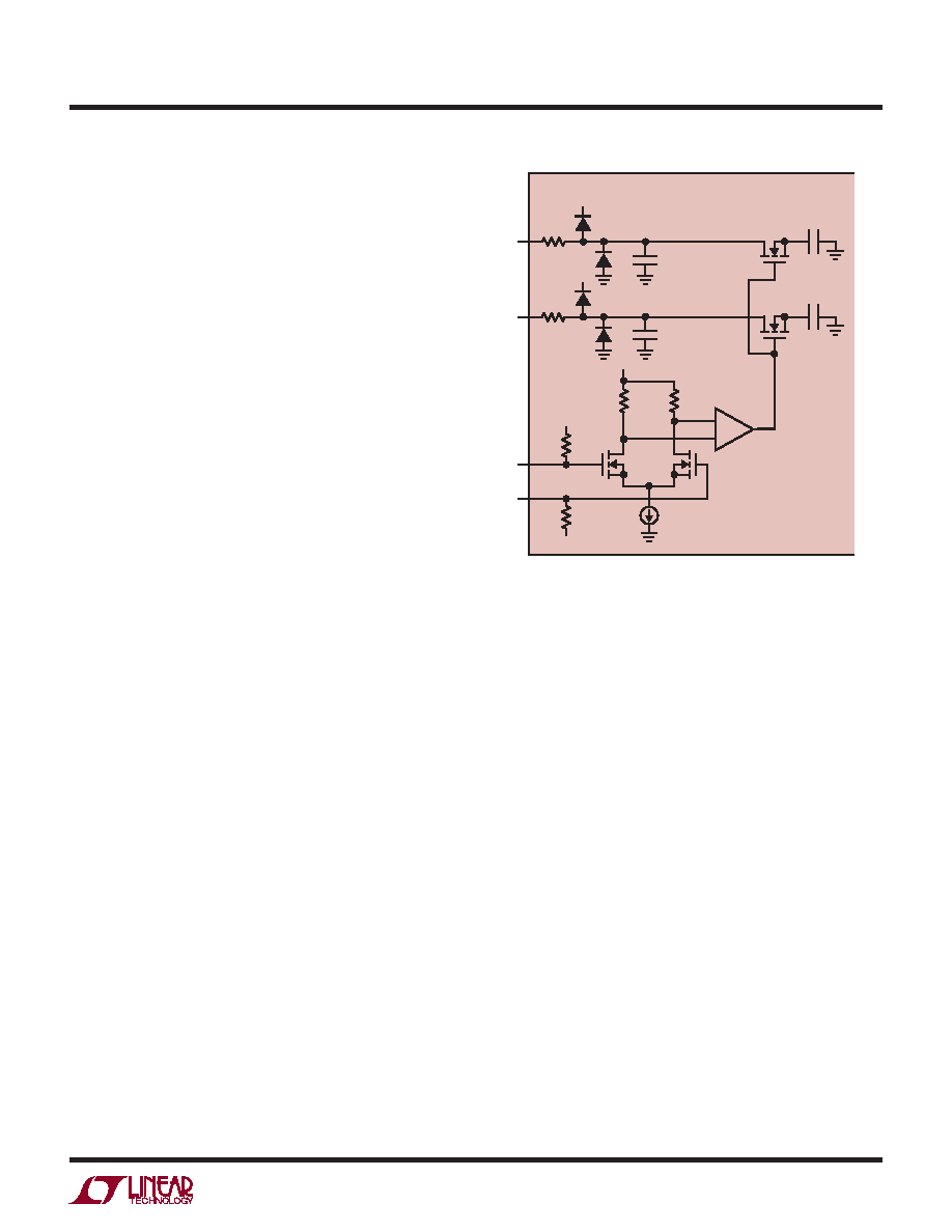
Figure 2 shows an equivalent circuit for the LTC2240-12
CMOS differential sample-and-hold. The analog inputs are
connected to the sampling capacitors (CSAMPLE) through
NMOS transistors. The capacitors shown attached to
each input (CPARASITIC) are the summation of all other
capacitance associated with each input.
During the sample phase when ENC is low, the transistors
connect the analog inputs to the sampling capacitors and
they charge to, and track the differential input voltage.
When ENC transitions from low to high, the sampled input
voltage is held on the sampling capacitors. During the
hold phase when ENC is high, the sampling capacitors are
disconnected from the input and the held voltage is passed
to the ADC core for processing. As ENC transitions from
high to low, the inputs are reconnected to the sampling
capacitors to acquire a new sample. Since the sampling
capacitors still hold the previous sample, a charging glitch
proportional to the change in voltage between samples will
be seen at this time. If the change between the last sample
and the new sample is small, the charging glitch seen at
the input will be small. If the input change is large, such
as the change seen with input frequencies near Nyquist,
then a larger charging glitch will be seen.
Common Mode Bias
For optimal performance the analog inputs should be
driven differentially. Each input should swing ±0.5V for the
2V range or ±0.25V for the 1V range, around a common
mode voltage of 1.25V. The VCM output pin (Pin 60) may
be used to provide the common mode bias level. VCM can
be tied directly to the center tap of a transformer to set
the DC input level or as a reference level to an op amp
differential driver circuit. The VCM pin must be bypassed to
ground close to the ADC with a 2.2μF or greater capacitor.
Figure 2. Equivalent Input Circuit
CSAMPLE
2pF
RON
14Ω
RON
14Ω
VDD
LTC2240-12
AIN
+
224012 F02
CSAMPLE
2pF
VDD
AIN
–
ENC–
ENC+
1.5V
6k
1.5V
6k
CPARASITIC
1.8pF
CPARASITIC
1.8pF
10Ω
相关PDF资料 |
PDF描述 |
|---|---|
| LTC2240IUP-10#PBF | IC ADC 10BIT 170MSPS 64-QFN |
| LTC2241IUP-10#PBF | IC ADC 10BIT 210MSPS 64-QFN |
| LTC2242IUP-10#PBF | IC ADC 10BIT 250MSPS 64-QFN |
| LTC2245IUH#TRPBF | IC ADC 14BIT 10MSPS 3V 32-QFN |
| LTC2249IUH#TRPBF | IC ADC 14BIT 80MSPS LP 32-QFN |
相关代理商/技术参数 |
参数描述 |
|---|---|
| LTC2240CUP-12-TR | 制造商:LINER 制造商全称:Linear Technology 功能描述:12-Bit, 170Msps ADC |
| LTC2240CUP-12-TRPBF | 制造商:LINER 制造商全称:Linear Technology 功能描述:12-Bit, 170Msps ADC |
| LTC2240IUP-10 | 制造商:LINER 制造商全称:Linear Technology 功能描述:10-Bit, 170Msps ADC |
| LTC2240IUP-10#PBF | 功能描述:IC ADC 10BIT 170MSPS 64-QFN RoHS:是 类别:集成电路 (IC) >> 数据采集 - 模数转换器 系列:- 标准包装:1 系列:- 位数:14 采样率(每秒):83k 数据接口:串行,并联 转换器数目:1 功率耗散(最大):95mW 电压电源:双 ± 工作温度:0°C ~ 70°C 安装类型:通孔 封装/外壳:28-DIP(0.600",15.24mm) 供应商设备封装:28-PDIP 包装:管件 输入数目和类型:1 个单端,双极 |
| LTC2240IUP-10#TRPBF | 功能描述:IC ADC 10BIT 170MSPS 64-QFN RoHS:是 类别:集成电路 (IC) >> 数据采集 - 模数转换器 系列:- 标准包装:1 系列:- 位数:14 采样率(每秒):83k 数据接口:串行,并联 转换器数目:1 功率耗散(最大):95mW 电压电源:双 ± 工作温度:0°C ~ 70°C 安装类型:通孔 封装/外壳:28-DIP(0.600",15.24mm) 供应商设备封装:28-PDIP 包装:管件 输入数目和类型:1 个单端,双极 |
发布紧急采购,3分钟左右您将得到回复。