- 您现在的位置:买卖IC网 > PDF目录10661 > LTC2256CUJ-14#PBF (Linear Technology)IC ADC 14BIT 25MSPS 1.8V 40-QFN PDF资料下载
参数资料
| 型号: | LTC2256CUJ-14#PBF |
| 厂商: | Linear Technology |
| 文件页数: | 16/34页 |
| 文件大小: | 0K |
| 描述: | IC ADC 14BIT 25MSPS 1.8V 40-QFN |
| 产品培训模块: | LTC2262 - Ultra Low Power High Speed ADCs |
| 标准包装: | 61 |
| 位数: | 14 |
| 采样率(每秒): | 25M |
| 数据接口: | 并联,串行,SPI |
| 转换器数目: | 1 |
| 功率耗散(最大): | 40mW |
| 电压电源: | 单电源 |
| 工作温度: | 0°C ~ 70°C |
| 安装类型: | 表面贴装 |
| 封装/外壳: | 40-WFQFN 裸露焊盘 |
| 供应商设备封装: | 40-QFN(6x6) |
| 包装: | 管件 |
| 输入数目和类型: | 1 个差分 |
| 配用: | DC718C-ND - DEMO QUIKEVAL-II DATA |
第1页第2页第3页第4页第5页第6页第7页第8页第9页第10页第11页第12页第13页第14页第15页当前第16页第17页第18页第19页第20页第21页第22页第23页第24页第25页第26页第27页第28页第29页第30页第31页第32页第33页第34页
23
225814fc
LTC2258-14
LTC2257-14/LTC2256-14
For more information www.linear.com/LTC2258-14
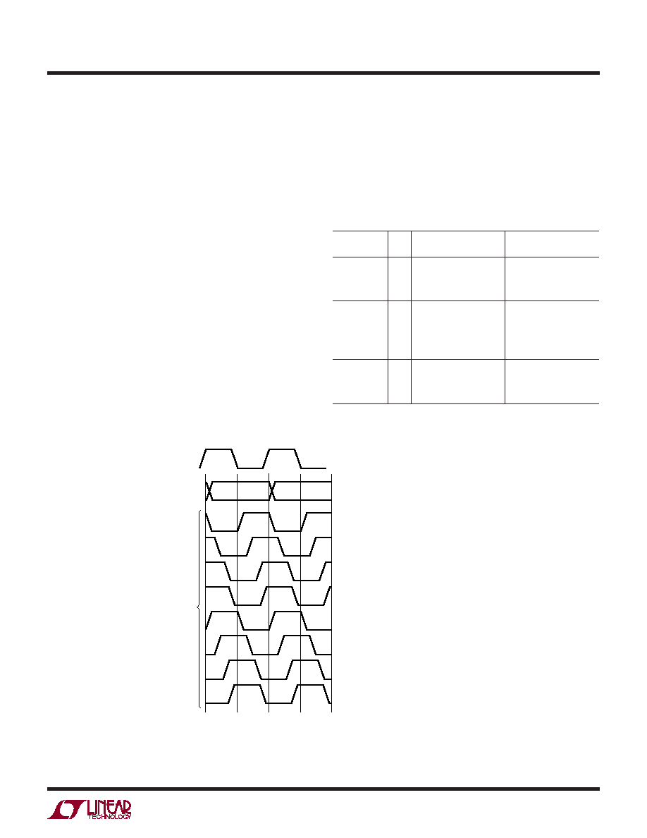
Phase Shifting the Output Clock
In full-rate CMOS mode the data output bits normally
change at the same time as the falling edge of CLKOUT+,
so the rising edge of CLKOUT+ can be used to latch the
output data. In double data rate CMOS and LVDS modes
the data output bits normally change at the same time as
the falling and rising edges of CLKOUT+. To allow adequate
setup-and-hold time when latching the data, the CLKOUT+
signal may need to be phase shifted relative to the data
output bits. Most FPGAs have this feature; this is generally
the best place to adjust the timing.
TheLTC2258-14/LTC2257-14/LTC2256-14canalsophase
shift the CLKOUT+/CLKOUT– signals by serially program-
ming mode control register A2. The output clock can be
shifted by 0°, 45°, 90° or 135°. To use the phase shifting
feature the clock duty cycle stabilizer must be turned
on. Another control register bit can invert the polarity of
CLKOUT+ and CLKOUT–, independently of the phase shift.
Thecombinationofthesetwofeaturesenablesphaseshifts
of 45° up to 315° (Figure 14).
DATA FORMAT
Table 1 shows the relationship between the analog input
voltage, the digital data output bits and the overflow bit.
By default the output data format is offset binary. The 2’s
complement format can be selected by serially program-
ming mode control register A4.
Table 1. Output Codes vs Input Voltage
AIN+ – AIN–
(2V Range)
OF
D13-D0
(OFFSET BINARY)
D13-D0
(2’s COMPLEMENT)
>1.000000V
+0.999878V
+0.999756V
1
0
11 1111 1111 1111
11 1111 1111 1110
01 1111 1111 1111
01 1111 1111 1110
+0.000122V
+0.000000V
–0.000122V
–0.000244V
0
10 0000 0000 0001
10 0000 0000 0000
01 1111 1111 1111
01 1111 1111 1110
00 0000 0000 0001
00 0000 0000 0000
11 1111 1111 1111
11 1111 1111 1110
–0.999878V
–1.000000V
≤–1.000000V
0
1
00 0000 0000 0001
00 0000 0000 0000
10 0000 0000 0001
10 0000 0000 0000
applicaTions inForMaTion
CLKOUT+
D0-D13, OF
PHASE
SHIFT
0°
45°
90°
135°
180°
225°
270°
315°
CLKINV
0
1
CLKPHASE1
MODE CONTROL BITS
0
1
0
1
CLKPHASE0
0
1
0
1
0
1
0
1
225814 F14
ENC+
Figure 14. Phase Shifting CLKOUT
相关PDF资料 |
PDF描述 |
|---|---|
| VI-B1X-IV-F4 | CONVERTER MOD DC/DC 5.2V 150W |
| MAX987EUK+TG103 | IC COMPARATOR R-R SOT23-5 |
| VI-B1X-IV-F3 | CONVERTER MOD DC/DC 5.2V 150W |
| AD7739BRUZ | IC ADC 24BIT 8-CH 24-TSSOP |
| MIC2550YML TR | IC USB TRANSCEIVER 16-MLF |
相关代理商/技术参数 |
参数描述 |
|---|---|
| LTC2256CUJ-14-TRPBF | 制造商:LINER 制造商全称:Linear Technology 功能描述:14-Bit, 65/40/25Msps Ultralow Power 1.8V ADCs |
| LTC2256IUJ-12#PBF | 功能描述:IC ADC 12BIT 25MSPS 1.8V 40-QFN RoHS:是 类别:集成电路 (IC) >> 数据采集 - 模数转换器 系列:- 标准包装:1,000 系列:- 位数:12 采样率(每秒):300k 数据接口:并联 转换器数目:1 功率耗散(最大):75mW 电压电源:单电源 工作温度:0°C ~ 70°C 安装类型:表面贴装 封装/外壳:24-SOIC(0.295",7.50mm 宽) 供应商设备封装:24-SOIC 包装:带卷 (TR) 输入数目和类型:1 个单端,单极;1 个单端,双极 |
| LTC2256IUJ-12#TRPBF | 功能描述:IC ADC 12BIT 25MSPS 1.8V 40-QFN RoHS:是 类别:集成电路 (IC) >> 数据采集 - 模数转换器 系列:- 标准包装:1,000 系列:- 位数:12 采样率(每秒):300k 数据接口:并联 转换器数目:1 功率耗散(最大):75mW 电压电源:单电源 工作温度:0°C ~ 70°C 安装类型:表面贴装 封装/外壳:24-SOIC(0.295",7.50mm 宽) 供应商设备封装:24-SOIC 包装:带卷 (TR) 输入数目和类型:1 个单端,单极;1 个单端,双极 |
| LTC2256IUJ-12-PBF | 制造商:LINER 制造商全称:Linear Technology 功能描述:12-Bit, 65/40/2 5Msps Ultralow Power 1.8V ADCs |
| LTC2256IUJ-12-TRPBF | 制造商:LINER 制造商全称:Linear Technology 功能描述:12-Bit, 65/40/2 5Msps Ultralow Power 1.8V ADCs |
发布紧急采购,3分钟左右您将得到回复。