- 您现在的位置:买卖IC网 > PDF目录10531 > LTC2290IUP#PBF (Linear Technology)IC ADC DUAL 12BIT 10MSPS 64QFN PDF资料下载
参数资料
| 型号: | LTC2290IUP#PBF |
| 厂商: | Linear Technology |
| 文件页数: | 7/24页 |
| 文件大小: | 0K |
| 描述: | IC ADC DUAL 12BIT 10MSPS 64QFN |
| 标准包装: | 40 |
| 位数: | 12 |
| 采样率(每秒): | 10M |
| 数据接口: | 并联 |
| 转换器数目: | 2 |
| 功率耗散(最大): | 138mW |
| 电压电源: | 单电源 |
| 工作温度: | -40°C ~ 85°C |
| 安装类型: | 表面贴装 |
| 封装/外壳: | 64-WFQFN 裸露焊盘 |
| 供应商设备封装: | 64-QFN(9x9) |
| 包装: | 管件 |
| 输入数目和类型: | 2 个单端,双极; 2 个差分, 双极 |
LTC2290
15
2290fa
APPLICATIO S I FOR ATIO
WU
UU
The difference amplifier generates the high and low refer-
ence for the ADC. High speed switching circuits are
connected to these outputs and they must be externally
bypassed. Each output has two pins. The multiple output
pins are needed to reduce package inductance. Bypass
capacitors must be connected as shown in Figure 6. Each
ADC channel has an independent reference with its own
bypass capacitors. The two channels can be used with the
same or different input ranges.
Other voltage ranges between the pin selectable ranges
can be programmed with two external resistors as shown
in Figure 7. An external reference can be used by applying
its output directly or through a resistor divider to SENSE.
It is not recommended to drive the SENSE pin with a logic
device. The SENSE pin should be tied to the appropriate
level as close to the converter as possible. If the SENSE pin
is driven externally, it should be bypassed to ground as
close to the device as possible with a 1
F ceramic capacitor.
For the best channel matching, connect an external reference
to SENSEA and SENSEB.
Figure 7. 1.5V Range ADC
VCM
SENSE
1.5V
0.75V
2.2
F
12k
1
F
12k
2290 F07
LTC2290
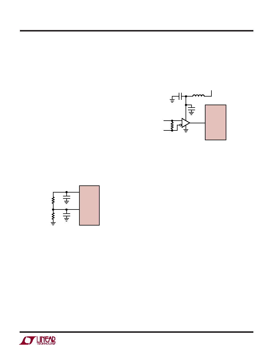
Driving the Clock Input
The CLK inputs can be driven directly with a CMOS or TTL
level signal. A differential clock can also be used along with
a low jitter CMOS converter before the CLK pin (Figure 8).
Figure 8. CLK Drive Using an LVDS or PECL to CMOS Converter
The noise performance of the LTC2290 can depend on the
clock signal quality as much as on the analog input. Any
noise present on the clock signal will result in additional
aperture jitter that will be RMS summed with the inherent
ADC aperture jitter.
It is recommended that CLKA and CLKB are shorted
together and driven by the same clock source. If a small
time delay is desired between when the two channels
sample the analog inputs, CLKA and CLKB can be driven
by two different signals. If this delay exceeds 1ns, the
performance of the part may degrade. CLKA and CLKB
should not be driven by asynchronous signals.
Input Range
The input range can be set based on the application. The
2V input range will provide the best signal-to-noise perfor-
mance while maintaining excellent SFDR. The 1V input
range will have better SFDR performance, but the SNR will
degrade by 3.8dB.
CLK
100
0.1
F
4.7
F
FERRITE
BEAD
CLEAN
SUPPLY
IF LVDS USE FIN1002 OR FIN1018.
FOR PECL, USE AZ1000ELT21 OR SIMILAR
2290 F08
LTC2290
相关PDF资料 |
PDF描述 |
|---|---|
| VI-BTR-MX-F4 | CONVERTER MOD DC/DC 7.5V 75W |
| ISL3171EIBZ | TXRX ESD 3.3V RS-485/422 8-SOIC |
| PT02SE-14-19P | CONN RCPT 19 POS BOX MNT W/PINS |
| AD7893BRZ-10 | IC ADC 12BIT SRL T/H LP 8SOIC |
| ISL3174EIBZ | TXRX ESD 3.3V RS-485/422 8-SOIC |
相关代理商/技术参数 |
参数描述 |
|---|---|
| LTC2290UP | 制造商:LINER 制造商全称:Linear Technology 功能描述:Dual 12-Bit, 10Msps Low Power 3V ADC |
| LTC2291 | 制造商:LINER 制造商全称:Linear Technology 功能描述:Dual 12-Bit, 65/40/25Msps Low Power 3V ADCs |
| LTC2291CUP | 制造商:Linear Technology 功能描述:ADC Dual Pipelined 25Msps 12-bit Parallel 64-Pin QFN EP |
| LTC2291CUP#PBF | 功能描述:IC ADC DUAL 12BIT 25MSPS 64QFN RoHS:是 类别:集成电路 (IC) >> 数据采集 - 模数转换器 系列:- 其它有关文件:TSA1204 View All Specifications 标准包装:1 系列:- 位数:12 采样率(每秒):20M 数据接口:并联 转换器数目:2 功率耗散(最大):155mW 电压电源:模拟和数字 工作温度:-40°C ~ 85°C 安装类型:表面贴装 封装/外壳:48-TQFP 供应商设备封装:48-TQFP(7x7) 包装:Digi-Reel® 输入数目和类型:4 个单端,单极;2 个差分,单极 产品目录页面:1156 (CN2011-ZH PDF) 其它名称:497-5435-6 |
| LTC2291CUP#TRPBF | 功能描述:IC ADC DUAL 12BIT 25MSPS 64QFN RoHS:是 类别:集成电路 (IC) >> 数据采集 - 模数转换器 系列:- 标准包装:1,000 系列:- 位数:12 采样率(每秒):300k 数据接口:并联 转换器数目:1 功率耗散(最大):75mW 电压电源:单电源 工作温度:0°C ~ 70°C 安装类型:表面贴装 封装/外壳:24-SOIC(0.295",7.50mm 宽) 供应商设备封装:24-SOIC 包装:带卷 (TR) 输入数目和类型:1 个单端,单极;1 个单端,双极 |
发布紧急采购,3分钟左右您将得到回复。