- 您现在的位置:买卖IC网 > PDF目录10252 > LTC2449IUHF#PBF (Linear Technology)IC ADC 24BIT HI SPEED 38QFN PDF资料下载
参数资料
| 型号: | LTC2449IUHF#PBF |
| 厂商: | Linear Technology |
| 文件页数: | 28/28页 |
| 文件大小: | 0K |
| 描述: | IC ADC 24BIT HI SPEED 38QFN |
| 标准包装: | 52 |
| 位数: | 24 |
| 采样率(每秒): | 8k |
| 数据接口: | MICROWIRE?,串行,SPI? |
| 转换器数目: | 1 |
| 功率耗散(最大): | 40mW |
| 电压电源: | 单电源 |
| 工作温度: | -40°C ~ 85°C |
| 安装类型: | 表面贴装 |
| 封装/外壳: | 38-WFQFN 裸露焊盘 |
| 供应商设备封装: | 38-QFN(5x7) |
| 包装: | 管件 |
| 输入数目和类型: | 16 个单端,双极;8 个差分,双极 |
| 配用: | DC742A-ND - BOARD DELTA SIGMA ADC LTC2449 |
第1页第2页第3页第4页第5页第6页第7页第8页第9页第10页第11页第12页第13页第14页第15页第16页第17页第18页第19页第20页第21页第22页第23页第24页第25页第26页第27页当前第28页
LTC2444/LTC2445/
LTC2448/LTC2449
9
2444589fb
LTC2448/LTC2449 convert the bipolar differential input
signal, VIN = IN+ – IN– (where IN+ and IN– are the selected
input channels), from – FS = – 0.5 VREF to +FS = 0.5 VREF
where VREF = REF+ – REF–. Outside this range, the con-
verter indicates the overrange or the underrange condition
using distinct output codes.
MUXOUT/ADCIN
There are two differences between the LTC2444/LTC2448
and the LTC2445/LTC2449. The first is the RMS noise
performance. For a given OSR, the LTC2445/LTC2449
noise level is approximately
√2 times lower (0.5 effective
bits)than that of the LTC2444/LTC2448.
The second difference is the LTC2445/LTC2449 includes
MUXOUT/ADCIN pins. These pins enable an external buffer
or gain block to be inserted between the output of the
multiplexer and the input to the ADC. Since the buffer is
driven by the output of the multiplexer, only one circuit is
required for all 16 input channels. Additionally, the trans-
parent calibration feature of the LTC244X family automati-
cally removes the offset errors of the external buffer.
In order to achieve optimum performance, the MUXOUT
and ADCIN pins should not be shorted together. In appli-
cations where the MUXOUT and ADCIN need to be shorted
together, the LTC2444/LTC2448 should be used because
the MUXOUT and ADCIN are internally connected for
optimum performance.
Output Data Format
The LTC2444/LTC2445/LTC2448/LTC2449 serial output
data stream is 32 bits long. The first 3 bits represent status
information indicating the sign and conversion state. The
next 24 bits are the conversion result, MSB first. The
remaining 5 bits are sub LSBs beyond the 24-bit level that
may be included in averaging or discarded without loss of
resolution. In the case of ultrahigh resolution modes,
more than 24 effective bits of performance are possible
(see Table 5). Under these conditions, sub LSBs are
included in the conversion result and represent useful
information beyond the 24-bit level. The third and fourth
bit together are also used to indicate an underrange
condition (the differential input voltage is below –FS) or an
overrange condition (the differential input voltage is above
+FS).
Bit 31 (first output bit) is the end of conversion (EOC)
indicator. This bit is available at the SDO pin during the
conversion and sleep states whenever the CS pin is LOW.
This bit is HIGH during the conversion and goes LOW
when the conversion is complete.
Bit 30 (second output bit) is a dummy bit (DMY) and is
always LOW.
Bit 29 (third output bit) is the conversion result sign indi-
cator (SIG). If VIN is >0, this bit is HIGH. If VIN is <0, this
bit is LOW.
Bit 28 (fourth output bit) is the most significant bit (MSB)
of the result. This bit in conjunction with Bit 29 also
provides the underrange or overrange indication. If both
Bit 29 and Bit 28 are HIGH, the differential input voltage is
above +FS. If both Bit 29 and Bit 28 are LOW, the
differential input voltage is below –FS.
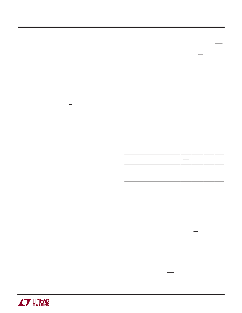
The function of these bits is summarized in Table 1.
Table 1. LTC2444/LTC2445/LTC2448/LTC2449 Status Bits
Bit 31
Bit 30 Bit 29 Bit 28
Input Range
EOC
DMY
SIG
MSB
VIN ≥ 0.5 VREF
00
1
0V
≤ VIN < 0.5 VREF
00
1
0
–0.5 VREF ≤ VIN < 0V
0
1
VIN < – 0.5 VREF
00
0
Bits 28-5 are the 24-bit conversion result MSB first.
Bit 5 is the least significant bit (LSB).
Bits 4-0 are sub LSBs below the 24-bit level. Bits 4-0 may
be included in averaging or discarded without loss of
resolution.
Data is shifted out of the SDO pin under control of the serial
clock (SCK), see Figure 3. Whenever CS is HIGH, SDO
remains high impedance and SCK is ignored.
In order to shift the conversion result out of the device, CS
must first be driven LOW. EOC is seen at the SDO pin of the
device once CS is pulled LOW. EOC changes real time from
HIGH to LOW at the completion of a conversion. This
signal may be used as an interrupt for an external
microcontroller. Bit 31 (EOC) can be captured on the first
rising edge of SCK. Bit 30 is shifted out of the device on the
APPLICATIO S I FOR ATIO
WU
U
相关PDF资料 |
PDF描述 |
|---|---|
| VE-26F-IU-S | CONVERTER MOD DC/DC 72V 200W |
| AD7829BRU | IC ADC 8BIT 8CH 2MSPS 28TSSOP |
| LTC2447IUHF#TRPBF | IC ADC 24BIT 8CH HI SPEED 38QFN |
| LTC1867CGN | IC ADC 16BIT 8CH 200KSPS 16SSOP |
| VE-22V-MX-F3 | CONVERTER MOD DC/DC 5.8V 75W |
相关代理商/技术参数 |
参数描述 |
|---|---|
| LTC2450CDC#PBF | 制造商:Linear Technology 功能描述:ADC Single Delta-Sigma 30sps 16-bit Serial 6-Pin DFN EP 制造商:Linear Technology 功能描述:ADC Single Delta-Sigma 0.03KSPS 16-Bit Serial 6-Pin DFN EP 制造商:Linear Technology 功能描述:ADC Single Delta-Sigma 0.03KSPS 16-Bit Serial 6-Pin DFN EP Bulk 制造商:Linear Technology 功能描述:ADC 16BIT 30SPS SPI DFN-6 制造商:Linear Technology 功能描述:ADC, 16BIT, 30SPS, SPI, DFN-6; Resolution (Bits):16bit; Sampling Rate:30SPS; Supply Voltage Type:Single; Supply Voltage Min:2.7V; Supply Voltage Max:5.5V; Supply Current:350A; Digital IC Case Style:DFN; No. of Pins:6 ;RoHS Compliant: Yes |
| LTC2450CDC#TRMPBF | 功能描述:IC ADC 16BIT DELTA SIG 6-DFN RoHS:是 类别:集成电路 (IC) >> 数据采集 - 模数转换器 系列:- 产品培训模块:Lead (SnPb) Finish for COTS Obsolescence Mitigation Program 标准包装:1 系列:- 位数:10 采样率(每秒):357k 数据接口:DSP,MICROWIRE?,QSPI?,串行,SPI? 转换器数目:1 功率耗散(最大):830µW 电压电源:单电源 工作温度:-40°C ~ 85°C 安装类型:表面贴装 封装/外壳:10-WFDFN 裸露焊盘 供应商设备封装:10-TDFN-EP(3x3) 包装:剪切带 (CT) 输入数目和类型:2 个单端,单极;2 个单端,双极;1 个差分,单极;1 个差分,双极 产品目录页面:1396 (CN2011-ZH PDF) 其它名称:MAX1395ETB+TCT |
| LTC2450CDC#TRPBF | 功能描述:IC ADC 16BIT DELTA SIG 6-DFN RoHS:是 类别:集成电路 (IC) >> 数据采集 - 模数转换器 系列:- 标准包装:2,500 系列:- 位数:16 采样率(每秒):15 数据接口:MICROWIRE?,串行,SPI? 转换器数目:1 功率耗散(最大):480µW 电压电源:单电源 工作温度:-40°C ~ 85°C 安装类型:表面贴装 封装/外壳:38-WFQFN 裸露焊盘 供应商设备封装:38-QFN(5x7) 包装:带卷 (TR) 输入数目和类型:16 个单端,双极;8 个差分,双极 配用:DC1011A-C-ND - BOARD DELTA SIGMA ADC LTC2494 |
| LTC2450CDC-1#PBF | 制造商:Linear Technology 功能描述:EASY-TO-USE, ULTRA-TINY 16-BIT DELTA SEGMA ADC 制造商:Linear Technology 功能描述:Bulk 制造商:Linear Technology 功能描述:ADC 16BIT DEL SIG 60HZ 6DF 制造商:Linear Technology 功能描述:ADC, 16BIT, 60SPS, SPI, DFN-6; Resolution (Bits):16bit; Sampling Rate:60SPS; Supply Voltage Type:Single; Supply Voltage Min:2.7V; Supply Voltage Max:5.5V; Supply Current:350A; Digital IC Case Style:DFN; No. of Pins:6 ;RoHS Compliant: Yes |
| LTC2450CDC-1#TRMPBF | 功能描述:IC ADC 16BIT DELTA SIG 6-DFN RoHS:是 类别:集成电路 (IC) >> 数据采集 - 模数转换器 系列:- 标准包装:1 系列:microPOWER™ 位数:8 采样率(每秒):1M 数据接口:串行,SPI? 转换器数目:1 功率耗散(最大):- 电压电源:模拟和数字 工作温度:-40°C ~ 125°C 安装类型:表面贴装 封装/外壳:24-VFQFN 裸露焊盘 供应商设备封装:24-VQFN 裸露焊盘(4x4) 包装:Digi-Reel® 输入数目和类型:8 个单端,单极 产品目录页面:892 (CN2011-ZH PDF) 其它名称:296-25851-6 |
发布紧急采购,3分钟左右您将得到回复。