参数资料
| 型号: | LTC2605CGN#PBF |
| 厂商: | Linear Technology |
| 文件页数: | 3/18页 |
| 文件大小: | 0K |
| 描述: | IC DAC 16BIT OCT I2C 16-SSOP |
| 标准包装: | 100 |
| 设置时间: | 10µs |
| 位数: | 16 |
| 数据接口: | I²C |
| 转换器数目: | 8 |
| 电压电源: | 单电源 |
| 功率耗散(最大): | 6mW |
| 工作温度: | 0°C ~ 70°C |
| 安装类型: | 表面贴装 |
| 封装/外壳: | 16-SSOP(0.154",3.90mm 宽) |
| 供应商设备封装: | 16-SSOP |
| 包装: | 管件 |
| 输出数目和类型: | 8 电压,单极 |
| 采样率(每秒): | * |
| 配用: | DC935A-ND - BOARD DAC LTC2605 |
LTC2605/LTC2615/LTC2625
11
2605fa
OPERATION
Power-On Reset
The LTC2605/LTC2615/LTC2625 clear the outputs to
zero-scale when power is rst applied, making system
initialization consistent and repeatable. The LTC2605-1/
LTC2615-1/LTC2625-1 set the voltage outputs to mid-scale
when power is rst applied.
For some applications, downstream circuits are active dur-
ing DAC power-up, and may be sensitive to nonzero outputs
from the DAC during this time. The LTC2605/LTC2615/
LTC2625 contain circuitry to reduce the power-on glitch:
the analog outputs typically rise less than 10mV above
zero-scale during power on if the power supply is ramped
to 5V in 1ms or more. In general, the glitch amplitude
decreases as the power supply ramp time is increased.
See Power-On Reset Glitch in the Typical Performance
Characteristics section.
Power Supply Sequencing
The voltage at REF (Pin 6) should be kept within the range
–0.3V ≤ VREF ≤ VCC + 0.3V (see Absolute Maximum Rat-
ings). Particular care should be taken to observe these
limits during power supply turn-on and turn-off sequences,
when the voltage at VCC (Pin 16) is in transition.
Transfer Function
The digital-to-analog transfer function is:
V
k
V
OUT IDEAL
N
REF
() =
2
where k is the decimal equivalent of the binary DAC input
code, N is the resolution and VREF is the voltage at REF
(Pin 6).
Serial Digital Interface
The LTC2605/LTC2615/LTC2625 communicate with a
host using the standard 2-wire digital interface. The Tim-
ing Diagram (Figure 1) shows the timing relationship of
the signals on the bus. The two bus lines, SDA and SCL,
must be high when the bus is not in use. External pull-up
resistors or current sources are required on these lines.
The value of these pull-up resistors is dependent on the
power supply and can be obtained from the I2C specica-
tions. For an I2C bus operating in the fast mode, an active
pull-up will be necessary if the bus capacitance is greater
than 200pF. The VCC power should not be removed from
the LTC2605/LTC2615/LTC2625 when the I2C bus is active
to avoid loading the I2C bus lines through the internal ESD
protection diodes.
The LTC2605/LTC2615/LTC2625 are receive-only (slave)
devices. The master can write to the LTC2605/LTC2615/
LTC2625. The LTC2605/LTC2615/LTC2625 do not respond
to a read from the master.
The START (S) and STOP (P) Conditions
When the bus is not in use, both SCL and SDA must be
high. A bus master signals the beginning of a communica-
tion to a slave device by transmitting a START condition. A
START condition is generated by transitioning SDA from
high to low while SCL is high.
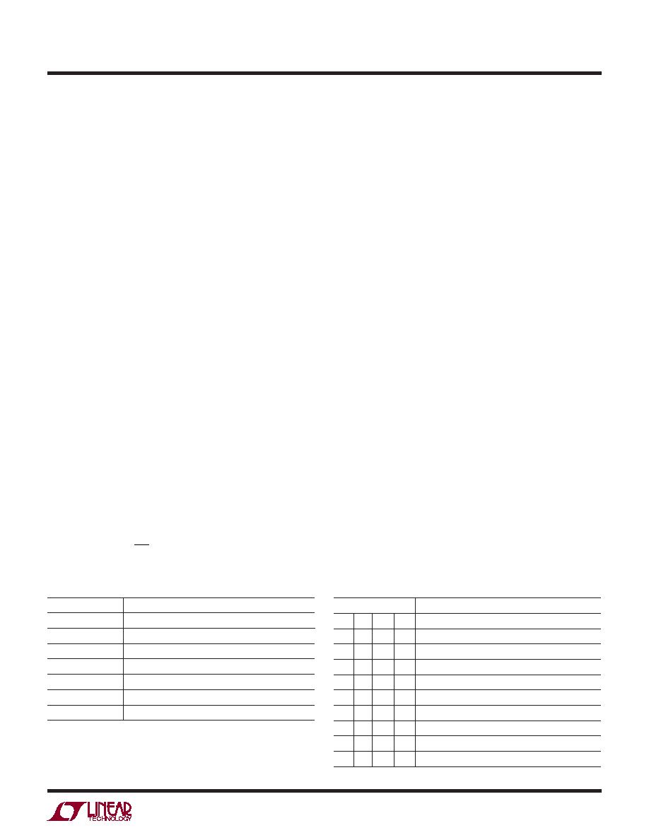
Table 1
COMMAND*
C3
C2
C1
C0
0
Write to Input Register n
0
1
Update (Power Up) DAC Register n
0
1
0
Write to Input Register n, Update (Power Up) All n
0
1
Write to and Update (Power Up) n
0
1
0
Power Down n
1
No Operation
*Address and command codes not shown are reserved and should not
be used.
ADDRESS (n)*
A3
A2
A1
A0
0
DAC A
0
1
DAC B
0
1
0
DAC C
0
1
DAC D
0
1
0
DAC E
0
1
0
1
DAC F
0
1
0
DAC G
0
1
DAC H
1
All DACs
相关PDF资料 |
PDF描述 |
|---|---|
| AD7564ARS-BREEL | IC DAC 12BIT QUAD 3.3V LP 28SSOP |
| SY88923AVKC TR | IC AMP POST 5V/3.3V 10-MSOP |
| VE-25P-IV-F2 | CONVERTER MOD DC/DC 13.8V 150W |
| SY88923AVKC | IC AMP POST 5V/3.3V 10-MSOP |
| VE-25N-IV-F1 | CONVERTER MOD DC/DC 18.5V 150W |
相关代理商/技术参数 |
参数描述 |
|---|---|
| LTC2605IGN#PBF | 功能描述:IC DAC 16BIT OCT I2C 16-SSOP RoHS:是 类别:集成电路 (IC) >> 数据采集 - 数模转换器 系列:- 产品培训模块:Data Converter Fundamentals DAC Architectures 标准包装:750 系列:- 设置时间:7µs 位数:16 数据接口:并联 转换器数目:1 电压电源:双 ± 功率耗散(最大):100mW 工作温度:0°C ~ 70°C 安装类型:表面贴装 封装/外壳:28-LCC(J 形引线) 供应商设备封装:28-PLCC(11.51x11.51) 包装:带卷 (TR) 输出数目和类型:1 电压,单极;1 电压,双极 采样率(每秒):143k |
| LTC2605IGN#TRPBF | 功能描述:IC DAC 16BIT OCT I2C 16-SSOP RoHS:是 类别:集成电路 (IC) >> 数据采集 - 数模转换器 系列:- 产品培训模块:Data Converter Fundamentals DAC Architectures 标准包装:750 系列:- 设置时间:7µs 位数:16 数据接口:并联 转换器数目:1 电压电源:双 ± 功率耗散(最大):100mW 工作温度:0°C ~ 70°C 安装类型:表面贴装 封装/外壳:28-LCC(J 形引线) 供应商设备封装:28-PLCC(11.51x11.51) 包装:带卷 (TR) 输出数目和类型:1 电压,单极;1 电压,双极 采样率(每秒):143k |
| LTC2605IGN-1#PBF | 功能描述:IC DAC 16BIT OCT I2C 16-SSOP RoHS:是 类别:集成电路 (IC) >> 数据采集 - 数模转换器 系列:- 产品培训模块:Lead (SnPb) Finish for COTS Obsolescence Mitigation Program 标准包装:50 系列:- 设置时间:4µs 位数:12 数据接口:串行 转换器数目:2 电压电源:单电源 功率耗散(最大):- 工作温度:-40°C ~ 85°C 安装类型:表面贴装 封装/外壳:8-TSSOP,8-MSOP(0.118",3.00mm 宽) 供应商设备封装:8-uMAX 包装:管件 输出数目和类型:2 电压,单极 采样率(每秒):* 产品目录页面:1398 (CN2011-ZH PDF) |
| LTC2605IGN-1#TRPBF | 功能描述:IC DAC 16BIT OCT I2C 16-SSOP RoHS:是 类别:集成电路 (IC) >> 数据采集 - 数模转换器 系列:- 产品培训模块:Data Converter Fundamentals DAC Architectures 标准包装:750 系列:- 设置时间:7µs 位数:16 数据接口:并联 转换器数目:1 电压电源:双 ± 功率耗散(最大):100mW 工作温度:0°C ~ 70°C 安装类型:表面贴装 封装/外壳:28-LCC(J 形引线) 供应商设备封装:28-PLCC(11.51x11.51) 包装:带卷 (TR) 输出数目和类型:1 电压,单极;1 电压,双极 采样率(每秒):143k |
| LTC2606CDD#PBF | 功能描述:IC DAC 16BIT I2C V-OUT 10-DFN RoHS:是 类别:集成电路 (IC) >> 数据采集 - 数模转换器 系列:- 产品培训模块:Lead (SnPb) Finish for COTS Obsolescence Mitigation Program 标准包装:50 系列:- 设置时间:4µs 位数:12 数据接口:串行 转换器数目:2 电压电源:单电源 功率耗散(最大):- 工作温度:-40°C ~ 85°C 安装类型:表面贴装 封装/外壳:8-TSSOP,8-MSOP(0.118",3.00mm 宽) 供应商设备封装:8-uMAX 包装:管件 输出数目和类型:2 电压,单极 采样率(每秒):* 产品目录页面:1398 (CN2011-ZH PDF) |
发布紧急采购,3分钟左右您将得到回复。