参数资料
| 型号: | LTC2625IGN-1#PBF |
| 厂商: | Linear Technology |
| 文件页数: | 14/18页 |
| 文件大小: | 0K |
| 描述: | IC DAC 12BIT R-R OCT 16SSOP |
| 标准包装: | 100 |
| 设置时间: | 7µs |
| 位数: | 12 |
| 数据接口: | 串行 |
| 转换器数目: | 8 |
| 电压电源: | 单电源 |
| 功率耗散(最大): | 6mW |
| 工作温度: | -40°C ~ 85°C |
| 安装类型: | 表面贴装 |
| 封装/外壳: | 16-SSOP(0.154",3.90mm 宽) |
| 供应商设备封装: | 16-SSOP |
| 包装: | 管件 |
| 输出数目和类型: | 8 电压,单极 |
| 采样率(每秒): | * |
| 产品目录页面: | 1351 (CN2011-ZH PDF) |
LTC2605/LTC2615/LTC2625
5
2605fa
TIMING CHARACTERISTICS The l denotes the specications which apply over the full operating temperature
range, otherwise specications are at TA = 25°C. See Figure 1. (Notes 8, 9)
SYMBOL
PARAMETER
CONDITIONS
MIN
TYP
MAX
UNITS
VCC = 2.7V to 5.5V
fSCL
SCL Clock Frequency
l
0
400
kHz
tHD(STA)
Hold Time (Repeated) Start Condition
l
0.6
μs
tLOW
Low Period of the SCL Clock Pin
l
1.3
μs
tHIGH
High Period of the SCL Clock Pin
l
0.6
μs
tSU(STA)
Set-Up Time for a Repeated Start Program
l
0.6
μs
tHD(DAT)
Data Hold Time
l
0
0.9
μs
tSU(DAT)
Data Set-Up Time
l
100
ns
tr
Rise Time of Both SDA and SCL Signals
(Note 7)
l 20 + 0.1CB
300
ns
tf
Fall Time of Both SDA and SCL Signals
(Note 7)
l 20 + 0.1CB
300
ns
tSU(STO)
Set-Up Time for Stop Condition
l
0.6
μs
tBUF
Bus Free Time Between a Stop and Start Condition
l
1.3
μs
Note 1: Stresses beyond those listed under Absolute Maximum Ratings
may cause permanent damage to the device. Exposure to any Absolute
Maximum Rating condition for extended periods may affect device
reliability and lifetime.
Note 2: Linearity and monotonicity are dened from code kL to code
2N – 1, where N is the resolution and kL is given by kL = 0.016(2N/VREF),
rounded to the nearest whole code. For VREF = 4.096V and N = 16,
kL = 256 and linearity is dened from code 256 to code 65,535.
Note 3: SDA, SCL at 0V or VCC, CA0, CA1 and CA2 oating.
Note 4: Inferred from measurement at code 256 (LTC2605/LTC2605-1),
code 64 (LTC2615/LTC2615-1) or code 16 (LTC2625/LTC2625-1) and at
full-scale.
Note 5: VCC = 5V, VREF = 4.096V. DAC is stepped 1/4-scale to 3/4-scale and
3/4-scale to 1/4-scale. Load is 2kΩ in parallel with 200pF to GND.
Note 6: VCC = 5V, VREF = 4.096V. DAC is stepped ±1LSB between half-scale
and half-scale – 1. Load is 2kΩ in parallel with 200pF to GND.
Note 7: CB = capacitance of one bus line in pF.
Note 8: All values refer to VIH(MIN) and VIL(MAX) levels.
Note 9: These specications apply to LTC2605/LTC2605-1,
LTC2615/LTC2615-1 and LTC2625/LTC2625-1.
Note 10: DC Crosstalk is measured with VCC = 5V and VREF = 4096V, with
the measured DAC at mid-scale, unless otherwise noted.
Note 11: RL = 2kΩ to GND or VCC.
Note 12: Guaranteed by design and not production tested.
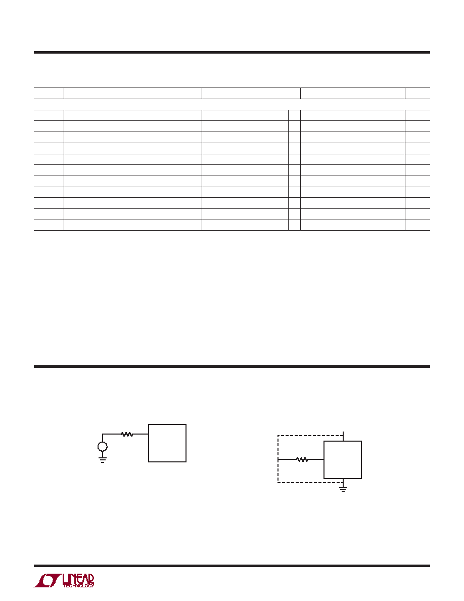
ELECTRICAL CHARACTERISTICS
Test Circuit 1
Test Circuit 2
VIH(CA
n)
/VIL(CA
n)
CAn
100Ω
2605 TC01
GND
RINH/RINL/RINF
VDD
2605 TC02
相关PDF资料 |
PDF描述 |
|---|---|
| GTC01CF-24-67P | CONN RCPT 19POS INLINE W/PINS |
| MS3450LS22-22S | CONN RCPT 4POS WALL MNT W/SCKT |
| D38999/24KB98SN | CONN RCPT 6POS JAM NUT W/SCKT |
| AD7845JPZ | IC DAC 12BIT MULT LC2MOS 28-PLCC |
| MS3124F20-41S | CONN RCPT 41POS JAM NUT W/SCKT |
相关代理商/技术参数 |
参数描述 |
|---|---|
| LTC2626CDD | 制造商:Linear Technology 功能描述:DAC 1-CH 12-bit 10-Pin DFN EP |
| LTC2626CDD#PBF | 功能描述:IC DAC 12BIT I2C V-OUT 10-DFN RoHS:是 类别:集成电路 (IC) >> 数据采集 - 数模转换器 系列:- 产品培训模块:Lead (SnPb) Finish for COTS Obsolescence Mitigation Program 标准包装:50 系列:- 设置时间:4µs 位数:12 数据接口:串行 转换器数目:2 电压电源:单电源 功率耗散(最大):- 工作温度:-40°C ~ 85°C 安装类型:表面贴装 封装/外壳:8-TSSOP,8-MSOP(0.118",3.00mm 宽) 供应商设备封装:8-uMAX 包装:管件 输出数目和类型:2 电压,单极 采样率(每秒):* 产品目录页面:1398 (CN2011-ZH PDF) |
| LTC2626CDD#TRPBF | 功能描述:IC DAC 12BIT I2C V-OUT 10-DFN RoHS:是 类别:集成电路 (IC) >> 数据采集 - 数模转换器 系列:- 产品培训模块:Data Converter Fundamentals DAC Architectures 设计资源:Unipolar, Precision DC Digital-to-Analog Conversion using AD5450/1/2/3 8-14-Bit DACs (CN0052) Precision, Bipolar, Configuration for AD5450/1/2/3 8-14bit Multiplying DACs (CN0053) AC Signal Processing Using AD5450/1/2/3 Current Output DACs (CN0054) Programmable Gain Element Using AD5450/1/2/3 Current Output DAC Family (CN0055) Single Supply Low Noise LED Current Source Driver Using a Current Output DAC in the Reverse Mode (CN0139) 标准包装:10,000 系列:- 设置时间:- 位数:12 数据接口:DSP,MICROWIRE?,QSPI?,串行,SPI? 转换器数目:1 电压电源:单电源 功率耗散(最大):- 工作温度:-40°C ~ 125°C 安装类型:表面贴装 封装/外壳:SOT-23-8 薄型,TSOT-23-8 供应商设备封装:TSOT-23-8 包装:带卷 (TR) 输出数目和类型:1 电流,单极;1 电流,双极 采样率(每秒):2.7M |
| LTC2626CDD-1#PBF | 功能描述:IC DAC 12BIT I2C V-OUT 10-DFN RoHS:是 类别:集成电路 (IC) >> 数据采集 - 数模转换器 系列:- 产品培训模块:Data Converter Fundamentals DAC Architectures 设计资源:Unipolar, Precision DC Digital-to-Analog Conversion using AD5450/1/2/3 8-14-Bit DACs (CN0052) Precision, Bipolar, Configuration for AD5450/1/2/3 8-14bit Multiplying DACs (CN0053) AC Signal Processing Using AD5450/1/2/3 Current Output DACs (CN0054) Programmable Gain Element Using AD5450/1/2/3 Current Output DAC Family (CN0055) Single Supply Low Noise LED Current Source Driver Using a Current Output DAC in the Reverse Mode (CN0139) 标准包装:10,000 系列:- 设置时间:- 位数:12 数据接口:DSP,MICROWIRE?,QSPI?,串行,SPI? 转换器数目:1 电压电源:单电源 功率耗散(最大):- 工作温度:-40°C ~ 125°C 安装类型:表面贴装 封装/外壳:SOT-23-8 薄型,TSOT-23-8 供应商设备封装:TSOT-23-8 包装:带卷 (TR) 输出数目和类型:1 电流,单极;1 电流,双极 采样率(每秒):2.7M |
| LTC2626CDD-1#TRPBF | 功能描述:IC DAC 12BIT I2C V-OUT 10-DFN RoHS:是 类别:集成电路 (IC) >> 数据采集 - 数模转换器 系列:- 产品培训模块:Data Converter Fundamentals DAC Architectures 设计资源:Unipolar, Precision DC Digital-to-Analog Conversion using AD5450/1/2/3 8-14-Bit DACs (CN0052) Precision, Bipolar, Configuration for AD5450/1/2/3 8-14bit Multiplying DACs (CN0053) AC Signal Processing Using AD5450/1/2/3 Current Output DACs (CN0054) Programmable Gain Element Using AD5450/1/2/3 Current Output DAC Family (CN0055) Single Supply Low Noise LED Current Source Driver Using a Current Output DAC in the Reverse Mode (CN0139) 标准包装:10,000 系列:- 设置时间:- 位数:12 数据接口:DSP,MICROWIRE?,QSPI?,串行,SPI? 转换器数目:1 电压电源:单电源 功率耗散(最大):- 工作温度:-40°C ~ 125°C 安装类型:表面贴装 封装/外壳:SOT-23-8 薄型,TSOT-23-8 供应商设备封装:TSOT-23-8 包装:带卷 (TR) 输出数目和类型:1 电流,单极;1 电流,双极 采样率(每秒):2.7M |
发布紧急采购,3分钟左右您将得到回复。