参数资料
| 型号: | LTC2625IGN-1#PBF |
| 厂商: | Linear Technology |
| 文件页数: | 2/18页 |
| 文件大小: | 0K |
| 描述: | IC DAC 12BIT R-R OCT 16SSOP |
| 标准包装: | 100 |
| 设置时间: | 7µs |
| 位数: | 12 |
| 数据接口: | 串行 |
| 转换器数目: | 8 |
| 电压电源: | 单电源 |
| 功率耗散(最大): | 6mW |
| 工作温度: | -40°C ~ 85°C |
| 安装类型: | 表面贴装 |
| 封装/外壳: | 16-SSOP(0.154",3.90mm 宽) |
| 供应商设备封装: | 16-SSOP |
| 包装: | 管件 |
| 输出数目和类型: | 8 电压,单极 |
| 采样率(每秒): | * |
| 产品目录页面: | 1351 (CN2011-ZH PDF) |
LTC2605/LTC2615/LTC2625
10
2605fa
PIN FUNCTIONS
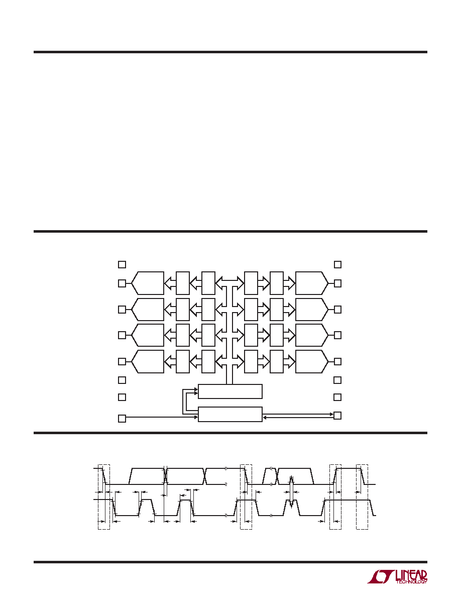
BLOCK DIAGRAM
TIMING DIAGRAM
GND (Pin 1): Analog Ground.
VOUT A to VOUT H (Pins 2-5 and 12-15): DAC Analog Volt-
age Output. The output range is 0V to VREF.
REF (Pin 6): Reference Voltage Input. 0V ≤ VREF ≤ VCC.
CA2 (Pin 7): Chip Address Bit 2. Tie this pin to VCC, GND
or leave it oating to select an I2C slave address for the
part (Table 2).
SCL (Pin 8): Serial Clock Input Pin. Data is shifted into
the SDA pin at the rising edges of the clock. This high
impedance pin requires a pull-up resistor or current
source to VCC.
SDA (Pin 9): Serial Data Bidirectional Pin. Data is shifted
into the SDA pin and acknowledged by the SDA pin. This
is a high impedance pin while data is shifted in. It is an
open-drain N-channel output during acknowledgment. This
pin requires a pull-up resistor or current source to VCC.
CA1 (Pin 10): Chip Address Bit 1. Tie this pin to VCC, GND
or leave it oating to select an I2C slave address for the
part (Table 2).
CA0 (Pin 11): Chip Address Bit 0. Tie this pin to VCC, GND
or leave it oating to select an I2C slave address for the
part (Table 2).
VCC (Pin 16): Supply Voltage Input. 2.7V ≤ VCC ≤ 5.5V.
2
15
1
GND
VOUT A
VOUT B
VOUT C
VOUT D
REF
CA2
SCL
VCC
VOUT H
VOUT G
VOUT F
VOUT E
CA0
CA1
SDA
2605 BD01
16
DAC A
3
14
4
13
5
7
6
8
10
11
9
12
2-WIRE INTERFACE
32-BIT SHIFT REGISTER
DAC
REGISTER
DAC
REGISTER
DAC
REGISTER
DAC
REGISTER
DAC
REGISTER
DAC
REGISTER
DAC
REGISTER
DAC
REGISTER
INPUT
REGISTER
INPUT
REGISTER
INPUT
REGISTER
INPUT
REGISTER
INPUT
REGISTER
INPUT
REGISTER
INPUT
REGISTER
INPUT
REGISTER
DAC H
DAC B
DAC G
DAC C
DAC F
DAC D
DAC E
SDA
tf
S
tr
tLOW
tHD(STA)
ALL VOLTAGE LEVELS REFER TO VIH(MIN) AND VIL(MAX) LEVELS
tHD(DAT)
tSU(DAT)
tSU(STA)
tHD(STA)
tSU(STO)
tSP
tBUF
tr
tf
tHIGH
SCL
S
P
S
2605 F01
Figure 1
相关PDF资料 |
PDF描述 |
|---|---|
| GTC01CF-24-67P | CONN RCPT 19POS INLINE W/PINS |
| MS3450LS22-22S | CONN RCPT 4POS WALL MNT W/SCKT |
| D38999/24KB98SN | CONN RCPT 6POS JAM NUT W/SCKT |
| AD7845JPZ | IC DAC 12BIT MULT LC2MOS 28-PLCC |
| MS3124F20-41S | CONN RCPT 41POS JAM NUT W/SCKT |
相关代理商/技术参数 |
参数描述 |
|---|---|
| LTC2626CDD | 制造商:Linear Technology 功能描述:DAC 1-CH 12-bit 10-Pin DFN EP |
| LTC2626CDD#PBF | 功能描述:IC DAC 12BIT I2C V-OUT 10-DFN RoHS:是 类别:集成电路 (IC) >> 数据采集 - 数模转换器 系列:- 产品培训模块:Lead (SnPb) Finish for COTS Obsolescence Mitigation Program 标准包装:50 系列:- 设置时间:4µs 位数:12 数据接口:串行 转换器数目:2 电压电源:单电源 功率耗散(最大):- 工作温度:-40°C ~ 85°C 安装类型:表面贴装 封装/外壳:8-TSSOP,8-MSOP(0.118",3.00mm 宽) 供应商设备封装:8-uMAX 包装:管件 输出数目和类型:2 电压,单极 采样率(每秒):* 产品目录页面:1398 (CN2011-ZH PDF) |
| LTC2626CDD#TRPBF | 功能描述:IC DAC 12BIT I2C V-OUT 10-DFN RoHS:是 类别:集成电路 (IC) >> 数据采集 - 数模转换器 系列:- 产品培训模块:Data Converter Fundamentals DAC Architectures 设计资源:Unipolar, Precision DC Digital-to-Analog Conversion using AD5450/1/2/3 8-14-Bit DACs (CN0052) Precision, Bipolar, Configuration for AD5450/1/2/3 8-14bit Multiplying DACs (CN0053) AC Signal Processing Using AD5450/1/2/3 Current Output DACs (CN0054) Programmable Gain Element Using AD5450/1/2/3 Current Output DAC Family (CN0055) Single Supply Low Noise LED Current Source Driver Using a Current Output DAC in the Reverse Mode (CN0139) 标准包装:10,000 系列:- 设置时间:- 位数:12 数据接口:DSP,MICROWIRE?,QSPI?,串行,SPI? 转换器数目:1 电压电源:单电源 功率耗散(最大):- 工作温度:-40°C ~ 125°C 安装类型:表面贴装 封装/外壳:SOT-23-8 薄型,TSOT-23-8 供应商设备封装:TSOT-23-8 包装:带卷 (TR) 输出数目和类型:1 电流,单极;1 电流,双极 采样率(每秒):2.7M |
| LTC2626CDD-1#PBF | 功能描述:IC DAC 12BIT I2C V-OUT 10-DFN RoHS:是 类别:集成电路 (IC) >> 数据采集 - 数模转换器 系列:- 产品培训模块:Data Converter Fundamentals DAC Architectures 设计资源:Unipolar, Precision DC Digital-to-Analog Conversion using AD5450/1/2/3 8-14-Bit DACs (CN0052) Precision, Bipolar, Configuration for AD5450/1/2/3 8-14bit Multiplying DACs (CN0053) AC Signal Processing Using AD5450/1/2/3 Current Output DACs (CN0054) Programmable Gain Element Using AD5450/1/2/3 Current Output DAC Family (CN0055) Single Supply Low Noise LED Current Source Driver Using a Current Output DAC in the Reverse Mode (CN0139) 标准包装:10,000 系列:- 设置时间:- 位数:12 数据接口:DSP,MICROWIRE?,QSPI?,串行,SPI? 转换器数目:1 电压电源:单电源 功率耗散(最大):- 工作温度:-40°C ~ 125°C 安装类型:表面贴装 封装/外壳:SOT-23-8 薄型,TSOT-23-8 供应商设备封装:TSOT-23-8 包装:带卷 (TR) 输出数目和类型:1 电流,单极;1 电流,双极 采样率(每秒):2.7M |
| LTC2626CDD-1#TRPBF | 功能描述:IC DAC 12BIT I2C V-OUT 10-DFN RoHS:是 类别:集成电路 (IC) >> 数据采集 - 数模转换器 系列:- 产品培训模块:Data Converter Fundamentals DAC Architectures 设计资源:Unipolar, Precision DC Digital-to-Analog Conversion using AD5450/1/2/3 8-14-Bit DACs (CN0052) Precision, Bipolar, Configuration for AD5450/1/2/3 8-14bit Multiplying DACs (CN0053) AC Signal Processing Using AD5450/1/2/3 Current Output DACs (CN0054) Programmable Gain Element Using AD5450/1/2/3 Current Output DAC Family (CN0055) Single Supply Low Noise LED Current Source Driver Using a Current Output DAC in the Reverse Mode (CN0139) 标准包装:10,000 系列:- 设置时间:- 位数:12 数据接口:DSP,MICROWIRE?,QSPI?,串行,SPI? 转换器数目:1 电压电源:单电源 功率耗散(最大):- 工作温度:-40°C ~ 125°C 安装类型:表面贴装 封装/外壳:SOT-23-8 薄型,TSOT-23-8 供应商设备封装:TSOT-23-8 包装:带卷 (TR) 输出数目和类型:1 电流,单极;1 电流,双极 采样率(每秒):2.7M |
发布紧急采购,3分钟左右您将得到回复。