参数资料
| 型号: | LTC2625IGN-1#PBF |
| 厂商: | Linear Technology |
| 文件页数: | 4/18页 |
| 文件大小: | 0K |
| 描述: | IC DAC 12BIT R-R OCT 16SSOP |
| 标准包装: | 100 |
| 设置时间: | 7µs |
| 位数: | 12 |
| 数据接口: | 串行 |
| 转换器数目: | 8 |
| 电压电源: | 单电源 |
| 功率耗散(最大): | 6mW |
| 工作温度: | -40°C ~ 85°C |
| 安装类型: | 表面贴装 |
| 封装/外壳: | 16-SSOP(0.154",3.90mm 宽) |
| 供应商设备封装: | 16-SSOP |
| 包装: | 管件 |
| 输出数目和类型: | 8 电压,单极 |
| 采样率(每秒): | * |
| 产品目录页面: | 1351 (CN2011-ZH PDF) |
LTC2605/LTC2615/LTC2625
12
2605fa
OPERATION
When the master has nished communicating with the
slave, it issues a STOP condition. A STOP condition is
generated by transitioning SDA from low to high while
SCL is high. The bus is then free for communication with
another I2C device.
Acknowledge
The Acknowledge signal is used for handshaking between
the master and the slave. An Acknowledge (active LOW)
generated by the slave lets the master know that the lat-
est byte of information was received. The Acknowledge
related clock pulse is generated by the master. The master
releases the SDA line (HIGH) during the Acknowledge
clock pulse. The slave-receiver must pull down the SDA
during the Acknowledge clock pulse so that it remains a
stable LOW during the HIGH period of this clock pulse.
The LTC2605/LTC2615/LTC2625 respond to a write by a
master in this manner. The LTC2605/LTC2615/LTC2625 do
not acknowledge a read (it retains SDA HIGH during the
period of the Acknowledge clock pulse).
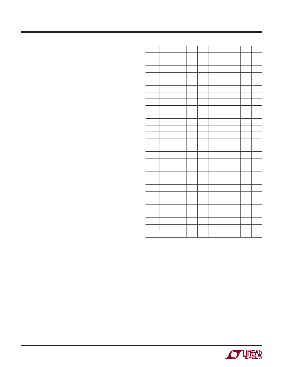
Chip Address
The state of CA0, CA1 and CA2 decides the slave address
of the part. The pins CA0, CA1 and CA2 can be each set to
any one of three states: VCC, GND or FLOAT. This results
in 27 selectable addresses for the part. The addresses
corresponding to the states of CA0, CA1 and CA2 and the
global address are shown in Table 2.
In addition to the address selected by the address pins,
the parts also respond to a global address. This address
allows a common write to all LTC2605, LTC2615 and
LTC2625 parts to be accomplished with one 3-byte write
transaction on the I2C bus. The global address is a 7-bit
hard-wired address and is not selectable by CA0, CA1 and
CA2. The maximum capacitive load allowed on the address
pins (CA0, CA1 and CA2) is 10pF.
Write Word Protocol
The master initiates communication with the LTC2605/
LTC2615/LTC2625 with a START condition and a 7-bit slave
address followed by the Write bit (W) = 0. The LTC2605/
LTC2615/LTC2625 acknowledges by pulling the SDA pin
Table 2. Slave Address Map
CA2
CA1
CA0
SA6
SA5
SA4
SA3
SA2
SA1
SA0
GND
0
1
0
GND
FLOAT
0010001
GND
VCC
0010010
GND
FLOAT
GND
0010011
GND
FLOAT FLOAT
0100000
GND
FLOAT
VCC
0100001
GND
VCC
GND
0100010
GND
VCC
FLOAT
0100011
GND
VCC
0110000
FLOAT
GND
0110001
FLOAT
GND
FLOAT
0110010
FLOAT
GND
VCC
0110011
FLOAT FLOAT
GND
1000000
FLOAT FLOAT FLOAT
1
0
1
FLOAT FLOAT
VCC
1000010
FLOAT
VCC
GND
1000011
FLOAT
VCC
FLOAT
1010000
FLOAT
VCC
1010001
VCC
GND
1010010
VCC
GND
FLOAT
1010011
VCC
GND
VCC
1100000
VCC
FLOAT
GND
1100001
VCC
FLOAT FLOAT
1100010
VCC
FLOAT
VCC
1100011
VCC
GND
1110000
VCC
FLOAT
1110001
VCC
1110010
GLOBAL ADDRESS
1
0
1
low at the 9th clock if the 7-bit slave address matches the
address of the parts (set by CA0, CA1 and CA2) or the
global address. The master then transmits three bytes of
data. The LTC2605/LTC2615/LTC2625 acknowledges each
byte of data by pulling the SDA line low at the 9th clock of
each data byte transmission. After receiving three complete
bytes of data, the LTC2605/LTC2615/LTC2625 executes the
command specied in the 24-bit input word.
If more than three data bytes are transmitted after a valid
7-bit slave address, the LTC2605/LTC2615/LTC2625 do not
acknowledge the extra bytes of data (SDA is high during
the 9th clock).
相关PDF资料 |
PDF描述 |
|---|---|
| GTC01CF-24-67P | CONN RCPT 19POS INLINE W/PINS |
| MS3450LS22-22S | CONN RCPT 4POS WALL MNT W/SCKT |
| D38999/24KB98SN | CONN RCPT 6POS JAM NUT W/SCKT |
| AD7845JPZ | IC DAC 12BIT MULT LC2MOS 28-PLCC |
| MS3124F20-41S | CONN RCPT 41POS JAM NUT W/SCKT |
相关代理商/技术参数 |
参数描述 |
|---|---|
| LTC2626CDD | 制造商:Linear Technology 功能描述:DAC 1-CH 12-bit 10-Pin DFN EP |
| LTC2626CDD#PBF | 功能描述:IC DAC 12BIT I2C V-OUT 10-DFN RoHS:是 类别:集成电路 (IC) >> 数据采集 - 数模转换器 系列:- 产品培训模块:Lead (SnPb) Finish for COTS Obsolescence Mitigation Program 标准包装:50 系列:- 设置时间:4µs 位数:12 数据接口:串行 转换器数目:2 电压电源:单电源 功率耗散(最大):- 工作温度:-40°C ~ 85°C 安装类型:表面贴装 封装/外壳:8-TSSOP,8-MSOP(0.118",3.00mm 宽) 供应商设备封装:8-uMAX 包装:管件 输出数目和类型:2 电压,单极 采样率(每秒):* 产品目录页面:1398 (CN2011-ZH PDF) |
| LTC2626CDD#TRPBF | 功能描述:IC DAC 12BIT I2C V-OUT 10-DFN RoHS:是 类别:集成电路 (IC) >> 数据采集 - 数模转换器 系列:- 产品培训模块:Data Converter Fundamentals DAC Architectures 设计资源:Unipolar, Precision DC Digital-to-Analog Conversion using AD5450/1/2/3 8-14-Bit DACs (CN0052) Precision, Bipolar, Configuration for AD5450/1/2/3 8-14bit Multiplying DACs (CN0053) AC Signal Processing Using AD5450/1/2/3 Current Output DACs (CN0054) Programmable Gain Element Using AD5450/1/2/3 Current Output DAC Family (CN0055) Single Supply Low Noise LED Current Source Driver Using a Current Output DAC in the Reverse Mode (CN0139) 标准包装:10,000 系列:- 设置时间:- 位数:12 数据接口:DSP,MICROWIRE?,QSPI?,串行,SPI? 转换器数目:1 电压电源:单电源 功率耗散(最大):- 工作温度:-40°C ~ 125°C 安装类型:表面贴装 封装/外壳:SOT-23-8 薄型,TSOT-23-8 供应商设备封装:TSOT-23-8 包装:带卷 (TR) 输出数目和类型:1 电流,单极;1 电流,双极 采样率(每秒):2.7M |
| LTC2626CDD-1#PBF | 功能描述:IC DAC 12BIT I2C V-OUT 10-DFN RoHS:是 类别:集成电路 (IC) >> 数据采集 - 数模转换器 系列:- 产品培训模块:Data Converter Fundamentals DAC Architectures 设计资源:Unipolar, Precision DC Digital-to-Analog Conversion using AD5450/1/2/3 8-14-Bit DACs (CN0052) Precision, Bipolar, Configuration for AD5450/1/2/3 8-14bit Multiplying DACs (CN0053) AC Signal Processing Using AD5450/1/2/3 Current Output DACs (CN0054) Programmable Gain Element Using AD5450/1/2/3 Current Output DAC Family (CN0055) Single Supply Low Noise LED Current Source Driver Using a Current Output DAC in the Reverse Mode (CN0139) 标准包装:10,000 系列:- 设置时间:- 位数:12 数据接口:DSP,MICROWIRE?,QSPI?,串行,SPI? 转换器数目:1 电压电源:单电源 功率耗散(最大):- 工作温度:-40°C ~ 125°C 安装类型:表面贴装 封装/外壳:SOT-23-8 薄型,TSOT-23-8 供应商设备封装:TSOT-23-8 包装:带卷 (TR) 输出数目和类型:1 电流,单极;1 电流,双极 采样率(每秒):2.7M |
| LTC2626CDD-1#TRPBF | 功能描述:IC DAC 12BIT I2C V-OUT 10-DFN RoHS:是 类别:集成电路 (IC) >> 数据采集 - 数模转换器 系列:- 产品培训模块:Data Converter Fundamentals DAC Architectures 设计资源:Unipolar, Precision DC Digital-to-Analog Conversion using AD5450/1/2/3 8-14-Bit DACs (CN0052) Precision, Bipolar, Configuration for AD5450/1/2/3 8-14bit Multiplying DACs (CN0053) AC Signal Processing Using AD5450/1/2/3 Current Output DACs (CN0054) Programmable Gain Element Using AD5450/1/2/3 Current Output DAC Family (CN0055) Single Supply Low Noise LED Current Source Driver Using a Current Output DAC in the Reverse Mode (CN0139) 标准包装:10,000 系列:- 设置时间:- 位数:12 数据接口:DSP,MICROWIRE?,QSPI?,串行,SPI? 转换器数目:1 电压电源:单电源 功率耗散(最大):- 工作温度:-40°C ~ 125°C 安装类型:表面贴装 封装/外壳:SOT-23-8 薄型,TSOT-23-8 供应商设备封装:TSOT-23-8 包装:带卷 (TR) 输出数目和类型:1 电流,单极;1 电流,双极 采样率(每秒):2.7M |
发布紧急采购,3分钟左右您将得到回复。