- 您现在的位置:买卖IC网 > PDF目录8607 > LTC2751AIUHF-16#TRPBF (Linear Technology)IC DAC 16BIT CUR OUT 38-QFN PDF资料下载
参数资料
| 型号: | LTC2751AIUHF-16#TRPBF |
| 厂商: | Linear Technology |
| 文件页数: | 5/22页 |
| 文件大小: | 0K |
| 描述: | IC DAC 16BIT CUR OUT 38-QFN |
| 产品培训模块: | LTC275x 18-Bit DAC |
| 标准包装: | 2,500 |
| 系列: | SoftSpan™ |
| 设置时间: | 2µs |
| 位数: | 16 |
| 数据接口: | 并联 |
| 转换器数目: | 1 |
| 电压电源: | 单电源 |
| 工作温度: | -40°C ~ 85°C |
| 安装类型: | 表面贴装 |
| 封装/外壳: | 38-WFQFN 裸露焊盘 |
| 供应商设备封装: | 38-QFN(5x7) |
| 包装: | 带卷 (TR) |
| 输出数目和类型: | 2 电流,单极;2 电流,双极 |
| 采样率(每秒): | * |
| 配用: | DC1110A-ND - BOARD DAC LTC2751-16 |
LTC2751
13
2751fa
operaTion
Table 1 shows the functions of the LTC2751.
Table 1. Write, Update and Read Functions
READ D/S
WR UPD
SPAN I/O
DATA I/O
0
-
Write to Input Register
0
1
-
Write/Update
(Transparent)
0
1
0
-
0
1
Update DAC Register Update DAC Register
0
1
0
Write to Input Register
-
0
1
0
1
Write/Update
(Transparent)
-
0
1
0
-
0
1
Update DAC register
Update DAC Register
1
0
X
0
-
Read Input Register
1
0
X
1
-
Read DAC Register
1
X
0
Read Input Register
-
1
X
1
Read DAC Register
-
X = Don’t Care
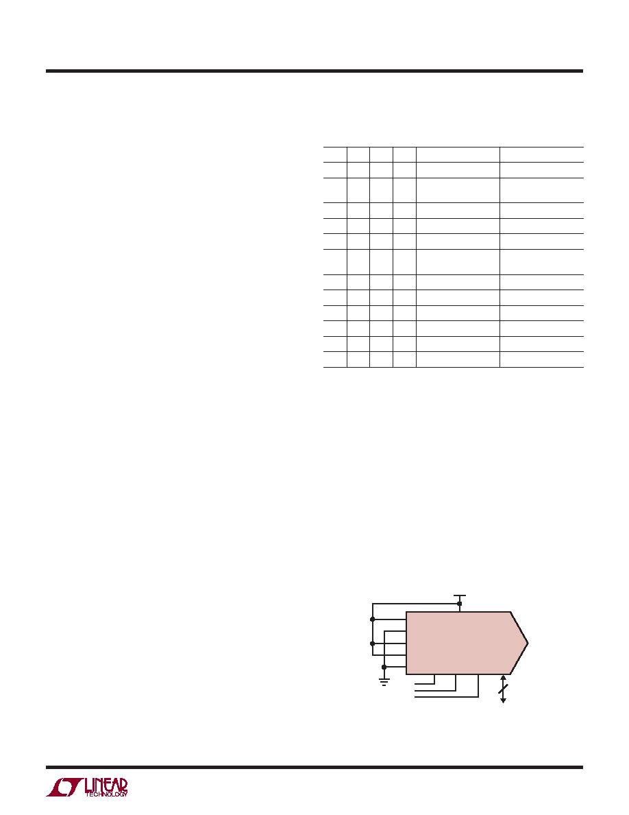
Manual Span Configuration
Multipleoutputrangesarenotneededinsomeapplications.
ToconfiguretheLTC2751forsingle-spanoperation,tiethe
MSPAN pin to VDD and the D/S pin to GND. The desired
output range is then specified by the span I/O pins (S0, S1
and S2) as usual, but the pins are programmed by tying
directly to GND or VDD (see Figure 1 and Table 2). In this
configuration, the part will initialize to the chosen output
range at power-up, with VOUT = 0V.
When configured for manual span operation, span pin
readback is disabled.
Write and Update Operations
The data input register is loaded directly from a 16-bit
microprocessor bus by holding the D/S pin low and then
pulsing the WR pin low. The second register (DAC regis-
ter) is loaded by pulsing the UPD pin high, which copies
the data held in the input register into the DAC register.
Note that updates always include both data and span; but
the DAC register values will not change unless the input
register values have been changed by writing.
Loadingthespaninputregisterisaccomplishedinasimilar
manner, by holding the D/S pin high and then bringing
the WR pin low. The span and data register structures
are the same except for the number of parallel bits—the
span registers have three bits, while the data registers
have 12, 14, or 16 bits.
To make both registers transparent for flowthrough mode,
tie WR low and UPD high. However, this defeats the de-
glitcher operation and output glitch impulse may increase.
ThedeglitcherisactivatedontherisingedgeoftheUPDpin.
The interface also allows the use of the input and DAC
registers in a master-slave, or edge-triggered, configura-
tion. This mode of operation occurs when WR and UPD
are tied together and driven by a single clock signal. The
data bits are loaded into the input register on the falling
edge of the clock and then loaded into the DAC register
on the rising edge.
The separation of data and span for write and read opera-
tions makes it possible to control both data and span on
one 16-bit wide data bus by allowing span pins S2 to S0
to share bus lines with the data LSBs (D2 to D0). Since
no write or read operation includes both span and data,
there cannot be a conflict.
The asynchronous clear pin resets the LTC2751 to 0V
(zero-, half- or quarter-scale code) in any output range.
CLR resets both the input and DAC data registers, while
leaving the span registers undisturbed.
These devices also have a power-on reset. If configured
for SoftSpan operation, the part initializes to zero scale in
the 0V to 5V output range. If configured for single-span
operation, the part initializes to the zero-volt code in the
chosen output range.
Figure 1. Configuring the LTC2751 for
Single-Span Operation (±10V Range)
LTC2751-16
MSPAN
S2
S1
S0
D/S
VDD
2751 F01
WR UPD READ
DATA I/O
16
VDD
相关PDF资料 |
PDF描述 |
|---|---|
| AD8332ARUZ-R7 | IC AMP VAR GAIN 2CHAN 28TSSOP |
| VI-24J-IV-F3 | CONVERTER MOD DC/DC 36V 150W |
| AD8332ARUZ-RL | IC AMP VAR GAIN 2CHAN 28TSSOP |
| AD5328ARU | IC DAC 12BIT OCTAL W/BUF 16TSSOP |
| AD8332ACPZ-RL | IC AMP VAR GAIN 2CHAN 32LFCSP |
相关代理商/技术参数 |
参数描述 |
|---|---|
| LTC2751BCUHF-16#PBF | 功能描述:IC DAC 16BIT CUR OUT 38-QFN RoHS:是 类别:集成电路 (IC) >> 数据采集 - 数模转换器 系列:SoftSpan™ 标准包装:47 系列:- 设置时间:2µs 位数:14 数据接口:并联 转换器数目:1 电压电源:单电源 功率耗散(最大):55µW 工作温度:-40°C ~ 85°C 安装类型:表面贴装 封装/外壳:28-SSOP(0.209",5.30mm 宽) 供应商设备封装:28-SSOP 包装:管件 输出数目和类型:1 电流,单极;1 电流,双极 采样率(每秒):* |
| LTC2751BCUHF-16#TRPBF | 功能描述:IC DAC 16BIT CUR OUT 38-QFN RoHS:是 类别:集成电路 (IC) >> 数据采集 - 数模转换器 系列:SoftSpan™ 标准包装:47 系列:- 设置时间:2µs 位数:14 数据接口:并联 转换器数目:1 电压电源:单电源 功率耗散(最大):55µW 工作温度:-40°C ~ 85°C 安装类型:表面贴装 封装/外壳:28-SSOP(0.209",5.30mm 宽) 供应商设备封装:28-SSOP 包装:管件 输出数目和类型:1 电流,单极;1 电流,双极 采样率(每秒):* |
| LTC2751BIUHF-16#PBF | 功能描述:IC DAC 16BIT CUR OUT 38-QFN RoHS:是 类别:集成电路 (IC) >> 数据采集 - 数模转换器 系列:SoftSpan™ 产品培训模块:Data Converter Fundamentals DAC Architectures 标准包装:750 系列:- 设置时间:7µs 位数:16 数据接口:并联 转换器数目:1 电压电源:双 ± 功率耗散(最大):100mW 工作温度:0°C ~ 70°C 安装类型:表面贴装 封装/外壳:28-LCC(J 形引线) 供应商设备封装:28-PLCC(11.51x11.51) 包装:带卷 (TR) 输出数目和类型:1 电压,单极;1 电压,双极 采样率(每秒):143k |
| LTC2751BIUHF-16#TRPBF | 功能描述:IC DAC 16BIT CUR OUT 38-QFN RoHS:是 类别:集成电路 (IC) >> 数据采集 - 数模转换器 系列:SoftSpan™ 产品培训模块:Data Converter Fundamentals DAC Architectures 标准包装:750 系列:- 设置时间:7µs 位数:16 数据接口:并联 转换器数目:1 电压电源:双 ± 功率耗散(最大):100mW 工作温度:0°C ~ 70°C 安装类型:表面贴装 封装/外壳:28-LCC(J 形引线) 供应商设备封装:28-PLCC(11.51x11.51) 包装:带卷 (TR) 输出数目和类型:1 电压,单极;1 电压,双极 采样率(每秒):143k |
| LTC2751CUHF-12#PBF | 功能描述:IC DAC 12BIT CUR OUT 38-QFN RoHS:是 类别:集成电路 (IC) >> 数据采集 - 数模转换器 系列:SoftSpan™ 产品培训模块:LTC263x 12-, 10-, and 8-Bit VOUT DAC Family 特色产品:LTC2636 - Octal 12-/10-/8-Bit SPI VOUT DACs with 10ppm/°C Reference 标准包装:91 系列:- 设置时间:4µs 位数:10 数据接口:MICROWIRE?,串行,SPI? 转换器数目:8 电压电源:单电源 功率耗散(最大):2.7mW 工作温度:-40°C ~ 85°C 安装类型:表面贴装 封装/外壳:14-WFDFN 裸露焊盘 供应商设备封装:14-DFN-EP(4x3) 包装:管件 输出数目和类型:8 电压,单极 采样率(每秒):* |
发布紧急采购,3分钟左右您将得到回复。