- 您现在的位置:买卖IC网 > PDF目录30769 > LTC3388IDD-1#PBF (LINEAR TECHNOLOGY CORP) 0.21 A SWITCHING REGULATOR, PDSO10 PDF资料下载
参数资料
| 型号: | LTC3388IDD-1#PBF |
| 厂商: | LINEAR TECHNOLOGY CORP |
| 元件分类: | 稳压器 |
| 英文描述: | 0.21 A SWITCHING REGULATOR, PDSO10 |
| 封装: | 3 X 3 MM, LEAD FREE, PLASTIC, MO-229WEED-2, DFN-10 |
| 文件页数: | 3/20页 |
| 文件大小: | 282K |
| 代理商: | LTC3388IDD-1#PBF |
LTC3388-1/LTC3388-3
11
338813f
OPERATION
The LTC3388-1/LTC3388-3 is an ultralow quiescent
current power supply designed to maintain a regulated
output voltage by means of a nanopower high efficiency
synchronous buck regulator.
Undervoltage Lockout (UVLO)
When the voltage on VIN rises above the UVLO rising
threshold the buck converter is enabled and charge is
transferred from the input capacitor to the output capacitor.
If VIN falls below the UVLO falling threshold the part will
re-enter UVLO. In UVLO the quiescent current is approxi-
mately 400nA and the buck converter is disabled.
Internal Rail Generation
Two internal rails, CAP and VIN2,aregeneratedfromVIN and
are used to drive the high side PMOS and low side NMOS
of the buck converter, respectively. Additionally the VIN2
rail serves as logic high for EN, STBY, and output voltage
select bits D0 and D1. The VIN2 rail is regulated at 4.6V
above GND while the CAP rail is regulated at 4.8V below
VIN. The VIN2 and CAP rails are not intended to be used
as external rails. Bypass capacitors are connected to the
CAP and VIN2 pins to serve as energy reservoirs for driving
the buck switches. When VIN is below 4.6V, VIN2 is equal
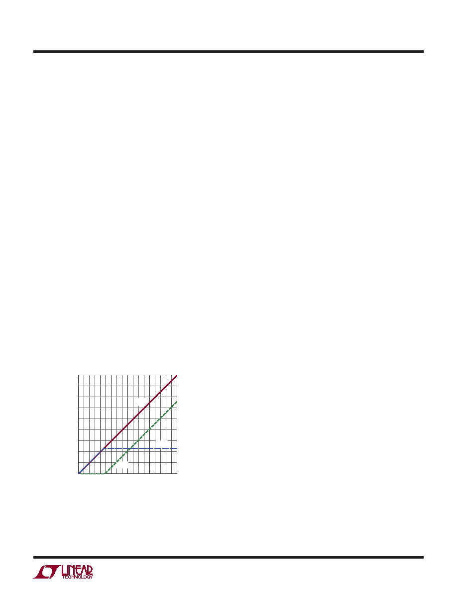
to VIN. CAP is at GND until VIN rises above 4.8V. Figure 1
shows the ideal VIN, VIN2 and CAP relationship.
Buck Operation
The buck regulator uses a hysteretic voltage algorithm
to control the output through internal feedback from the
VOUT sense pin. The buck converter charges an output
capacitor through an inductor to a value slightly higher than
the regulation point. It does this by ramping the inductor
current up to 150mA through an internal PMOS switch
and then ramping it down to 0mA through an internal
NMOS switch. This efficiently delivers energy to the output
capacitor. The ramp rate is determined by VIN, VOUT, and
the inductor value. When the buck brings the output volt-
age into regulation the converter enters a low quiescent
current sleep state that monitors the output voltage with
a sleep comparator. During this operating mode load cur-
rent is provided by the buck output capacitor. When the
output voltage falls below the regulation point the buck
regulator wakes up and the cycle repeats. This hysteretic
method of providing a regulated output reduces losses
associated with FET switching and maintains an output
at light loads. The buck delivers a minimum of 50mA of
average load current when it is switching.
When the sleep comparator signals that the output has
reached the sleep threshold the buck converter may be
in the middle of a cycle with current still flowing through
the inductor. Normally both synchronous switches would
turn off and the current in the inductor would freewheel
to zero through the NMOS body diode. The LTC3388-1/
LTC3388-3 keeps the NMOS switch on during this time to
prevent the conduction loss that would occur in the diode
if the NMOS were off. If the PMOS is on when the sleep
comparator trips, the NMOS will turn on immediately in
order to ramp down the current. If the NMOS is on it will
be kept on until the current reaches zero.
Though the quiescent current when the buck is switching
is much greater than the sleep quiescent current, it is still
a small percentage of the average inductor current which
results in high efficiency over most load conditions. The
buck operates only when the output voltage discharges
to the sleep falling threshold. Thus, the buck operating
quiescent current is averaged with the low sleep quiescent
current. This allows the converter to remain very efficient
at loads as low as 10μA.
Figure 1. Ideal VIN, VIN2 and CAP Relationship
VIN (V)
0
VOL
TAGE
(V)
18
16
14
12
10
8
6
4
2
0
338813 F01
10
515
VIN
VIN2
CAP
相关PDF资料 |
PDF描述 |
|---|---|
| LTC3388IMSE-1#PBF | 0.21 A SWITCHING REGULATOR, PDSO10 |
| LTC3388EDD-1#PBF | 0.21 A SWITCHING REGULATOR, PDSO10 |
| LTC3388IMSE-3#TRPBF | 0.21 A SWITCHING REGULATOR, PDSO10 |
| LTC3388EDD-1#TRPBF | 0.21 A SWITCHING REGULATOR, PDSO10 |
| LTC3388EMSE-1#TRPBF | 0.21 A SWITCHING REGULATOR, PDSO10 |
相关代理商/技术参数 |
参数描述 |
|---|---|
| LTC3388IDD-3 | 制造商:Linear Technology 功能描述: |
| LTC3388IDD-3#PBF | 功能描述:IC REG BUCK SYNC 50MA 10DFN RoHS:是 类别:集成电路 (IC) >> PMIC - 稳压器 - DC DC 开关稳压器 系列:- 标准包装:2,500 系列:- 类型:降压(降压) 输出类型:固定 输出数:1 输出电压:1.2V,1.5V,1.8V,2.5V 输入电压:2.7 V ~ 20 V PWM 型:- 频率 - 开关:- 电流 - 输出:50mA 同步整流器:是 工作温度:-40°C ~ 125°C 安装类型:表面贴装 封装/外壳:10-TFSOP,10-MSOP(0.118",3.00mm 宽)裸露焊盘 包装:带卷 (TR) 供应商设备封装:10-MSOP 裸露焊盘 |
| LTC3388IDD-3#TRPBF | 功能描述:IC REG BUCK SYNC 50MA 10DFN RoHS:是 类别:集成电路 (IC) >> PMIC - 稳压器 - DC DC 开关稳压器 系列:- 标准包装:2,500 系列:- 类型:降压(降压) 输出类型:固定 输出数:1 输出电压:1.2V,1.5V,1.8V,2.5V 输入电压:2.7 V ~ 20 V PWM 型:- 频率 - 开关:- 电流 - 输出:50mA 同步整流器:是 工作温度:-40°C ~ 125°C 安装类型:表面贴装 封装/外壳:10-TFSOP,10-MSOP(0.118",3.00mm 宽)裸露焊盘 包装:带卷 (TR) 供应商设备封装:10-MSOP 裸露焊盘 |
| LTC3388IMSE-1#PBF | 功能描述:IC REG BUCK SYNC 50MA 10MSOP RoHS:是 类别:集成电路 (IC) >> PMIC - 稳压器 - DC DC 开关稳压器 系列:- 标准包装:2,500 系列:- 类型:降压(降压) 输出类型:固定 输出数:1 输出电压:1.2V,1.5V,1.8V,2.5V 输入电压:2.7 V ~ 20 V PWM 型:- 频率 - 开关:- 电流 - 输出:50mA 同步整流器:是 工作温度:-40°C ~ 125°C 安装类型:表面贴装 封装/外壳:10-TFSOP,10-MSOP(0.118",3.00mm 宽)裸露焊盘 包装:带卷 (TR) 供应商设备封装:10-MSOP 裸露焊盘 |
| LTC3388IMSE-1#TRPBF | 功能描述:IC REG BUCK SYNC 50MA 10MSOP RoHS:是 类别:集成电路 (IC) >> PMIC - 稳压器 - DC DC 开关稳压器 系列:- 标准包装:2,500 系列:- 类型:降压(降压) 输出类型:固定 输出数:1 输出电压:1.2V,1.5V,1.8V,2.5V 输入电压:2.7 V ~ 20 V PWM 型:- 频率 - 开关:- 电流 - 输出:50mA 同步整流器:是 工作温度:-40°C ~ 125°C 安装类型:表面贴装 封装/外壳:10-TFSOP,10-MSOP(0.118",3.00mm 宽)裸露焊盘 包装:带卷 (TR) 供应商设备封装:10-MSOP 裸露焊盘 |
发布紧急采购,3分钟左右您将得到回复。