- 您现在的位置:买卖IC网 > PDF目录13082 > LTC3408EDD#PBF (Linear Technology)IC REG BUCK W/BYPASS TXRX 8-DFN PDF资料下载
参数资料
| 型号: | LTC3408EDD#PBF |
| 厂商: | Linear Technology |
| 文件页数: | 7/12页 |
| 文件大小: | 0K |
| 描述: | IC REG BUCK W/BYPASS TXRX 8-DFN |
| 标准包装: | 121 |
| 应用: | 转换器,WCDMA 功率放大器应用 |
| 输入电压: | 2.5 V ~ 5 V |
| 输出数: | 1 |
| 输出电压: | 0.3 V ~ 3.5 V |
| 工作温度: | -40°C ~ 85°C |
| 安装类型: | 表面贴装 |
| 封装/外壳: | 8-WFDFN 裸露焊盘 |
| 供应商设备封装: | 8-DFN-EP(3x3) |
| 包装: | 管件 |
�� �
�
�LTC3408�
�OPERATIO�
�(Refer� to� Functional� Diagram)�
�off� and� on� the� bypass� P-channel� MOSFET� with� a� frequency�
�of� approximately� 50kHz� to� 100kHz� at� 1.6A� peak� current.�
�This� will� continue� until� the� short� is� removed.� While� the�
�bypass� P-channel� MOSFET� is� pulsing� intermittently,� the�
�inherent� current� limit� of� the� step-down� regulator� limits� its�
�peak� current� to� about� 1A.�
�Dropout� Operation�
�If� the� reference� voltage� would� cause� V� OUT� to� exceed� V� IN� ,�
�the� LTC3408� enters� dropout� operation.� During� dropout,�
�the� main� switch� remains� on� continuously� and� operates� at�
�100%� duty� cycle.� If� the� voltage� at� REF� is� less� than� 1.2V,� the�
�bypass� P-channel� MOSFET� will� stay� off� even� in� dropout�
�operation.� The� output� voltage� is� then� determined� by� the�
�input� voltage� minus� the� voltage� drop� across� the� main� switch�
�and� the� inductor.� If� the� voltage� at� REF� is� greater� than� 1.2V,�
�1200�
�1000�
�but� less� than� V� IN� /3,� the� bypass� P-channel� MOSFET� will� be�
�on,� but� the� main� switch� will� be� off.� For� best� performance�
�and� lowest� voltage� drop� from� V� IN� to� V� OUT� ,� always� ensure�
�that� the� REF� voltage� is� greater� than� both� 1.2V� and� V� IN� /3.�
�An� important� detail� to� remember� is� that� at� low� input�
�supply� voltages,� the� R� DS(ON)� of� the� P-channel� switch�
�increases� (see� Typical� Performance� Characteristics).�
�Therefore,� the� user� should� calculate� the� power� dissipa-�
�tion� when� the� LTC3408� is� used� at� 100%� duty� cycle� with�
�low� input� voltage� (See� Thermal� Considerations� in� the�
�Applications� Information� section).�
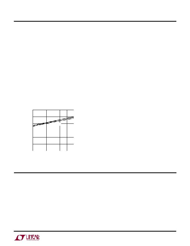
�Low� Supply� Operation�
�The� LTC3408� will� operate� with� input� supply� voltages� as�
�low� as� 2.5V,� but� the� maximum� allowable� output� current� is�
�reducedatthislowvoltage.Figure2showsthereduction�
�in� the� maximum� output� current� as� a� function� of� input�
�voltage� for� various� output� voltages.�
�800�
�600�
�400�
�200�
�V� OUT� = 1.8V�
�V� OUT� = 1.5V�
�V� OUT� = 2.5V�
�Slope� Compensation� and� Inductor� Peak� Current�
�Slope� compensation� provides� stability� in� constant� fre-�
�quency� architectures� by� preventing� subharmonic� oscilla-�
�tions� at� high� duty� cycles.� It� is� accomplished� internally� by�
�adding� a� compensating� ramp� to� the� inductor� current�
�signal� at� duty� cycles� in� excess� of� 40%.� Normally,� this�
�results� in� a� reduction� of� maximum� inductor� peak� current�
�0�
�2.5�
�3.0�
�3.5� 4.0� 4.5�
�5.0�
�5.5�
�for� duty� cycles� >� 40%.� However,� the� LTC3408� uses� a�
�SUPPLY� VOLTAGE� (V)�
�3408� F02�
�Figure� 2.� Maximum� Output� Current� vs� Input� Voltage�
�APPLICATIO� S� I� FOR� ATIO�
�The� basic� LTC3408� application� circuit� is� shown� in� Fig-�
�ure� 1.� External� component� selection� is� driven� by� the� load�
�requirement� and� begins� with� the� selection� of� L� followed� by�
�C� IN� and� C� OUT� .�
�Inductor� Selection�
�patent-pending� scheme� that� counteracts� this� compensat-�
�ing� ramp,� which� allows� the� maximum� inductor� peak�
�current� to� remain� unaffected� throughout� all� duty� cycles.�
�currents.� As� Equation� 1� shows,� a� greater� difference� be-�
�tween� V� IN� and� V� OUT� produces� a� larger� ripple� current.�
�Where� these� voltages� are� subject� to� change,� the� highest�
�V� IN� and� lowest� V� OUT� will� determine� the� maximum� ripple�
�current.� A� reasonable� starting� point� for� setting� ripple�
�current� is� I� L� =� 120mA� (20%� of� the� maximum� load,� 600mA).�
�V� OUT� ?� 1� –� OUT� ?�
�Formostapplications,thevalueoftheinductorwillfallin�
�the� range� of� 4� μ� H� to� 6� μ� H.� Its� value� is� chosen� based� on� the�
�desired� ripple� current.� Large� value� inductors� lower� ripple�
�current� and� small� value� inductors� result� in� higher� ripple�
�?� I� L� =�
�1�
�(� f� )(� L� )�
�?� V� ?�
�?� V� IN� ?�
�(1)�
�3408f�
�7�
�相关PDF资料 |
PDF描述 |
|---|---|
| MIC2954-02WT | IC REG LDO 5V .25A TO-220-3 |
| MIC5239-2.5YMM | IC REG LDO 2.5V .5A 8-MSOP |
| 1812-473J | INDUCTOR UNSHIELDED 47UH SMD |
| LTC3408EDD | IC REG BUCK W/BYPASS TXRX 8-DFN |
| MIC5239-1.8YMM | IC REG LDO 1.8V .5A 8-MSOP |
相关代理商/技术参数 |
参数描述 |
|---|---|
| LTC3409 | 制造商:LINER 制造商全称:Linear Technology 功能描述:600mA Low Vin Buck Regulator in 3mm x 3mm DFN |
| LTC3409A | 制造商:LINER 制造商全称:Linear Technology 功能描述:600mA Low VIN Buck Regulator in 3mm × 3mm DFN |
| LTC3409AEDD | 制造商:LINER 制造商全称:Linear Technology 功能描述:600mA Low VIN Buck Regulator in 3mm × 3mm DFN |
| LTC3409AEDD#PBF | 功能描述:IC REG BUCK SYNC ADJ 0.6A 8DFN RoHS:是 类别:集成电路 (IC) >> PMIC - 稳压器 - DC DC 开关稳压器 系列:- 标准包装:2,500 系列:- 类型:升压(升压) 输出类型:可调式 输出数:1 输出电压:1.24 V ~ 30 V 输入电压:1.5 V ~ 12 V PWM 型:电流模式,混合 频率 - 开关:600kHz 电流 - 输出:500mA 同步整流器:无 工作温度:-40°C ~ 85°C 安装类型:表面贴装 封装/外壳:8-SOIC(0.154",3.90mm 宽) 包装:带卷 (TR) 供应商设备封装:8-SOIC |
| LTC3409AEDD#TRPBF | 功能描述:IC REG BUCK SYNC ADJ 0.6A 8DFN RoHS:是 类别:集成电路 (IC) >> PMIC - 稳压器 - DC DC 开关稳压器 系列:- 标准包装:2,500 系列:- 类型:升压(升压) 输出类型:可调式 输出数:1 输出电压:1.24 V ~ 30 V 输入电压:1.5 V ~ 12 V PWM 型:电流模式,混合 频率 - 开关:600kHz 电流 - 输出:500mA 同步整流器:无 工作温度:-40°C ~ 85°C 安装类型:表面贴装 封装/外壳:8-SOIC(0.154",3.90mm 宽) 包装:带卷 (TR) 供应商设备封装:8-SOIC |
发布紧急采购,3分钟左右您将得到回复。