- 您现在的位置:买卖IC网 > PDF目录13082 > LTC3408EDD#PBF (Linear Technology)IC REG BUCK W/BYPASS TXRX 8-DFN PDF资料下载
参数资料
| 型号: | LTC3408EDD#PBF |
| 厂商: | Linear Technology |
| 文件页数: | 9/12页 |
| 文件大小: | 0K |
| 描述: | IC REG BUCK W/BYPASS TXRX 8-DFN |
| 标准包装: | 121 |
| 应用: | 转换器,WCDMA 功率放大器应用 |
| 输入电压: | 2.5 V ~ 5 V |
| 输出数: | 1 |
| 输出电压: | 0.3 V ~ 3.5 V |
| 工作温度: | -40°C ~ 85°C |
| 安装类型: | 表面贴装 |
| 封装/外壳: | 8-WFDFN 裸露焊盘 |
| 供应商设备封装: | 8-DFN-EP(3x3) |
| 包装: | 管件 |
�� �
�
�LTC3408�
�APPLICATIO� S� I� FOR� ATIO�
�forced� continuous� mode,� the� LTC3408� will� actually� pull�
�current� from� the� output� until� the� command� from� V� REF� is�
�satisfied.� On� alternate� half� cyles,� this� current� actually� exits�
�the� V� IN� terminal,� potentially� causing� a� rise� in� V� IN� and�
�forcing� current� into� the� battery.� To� prevent� deterioration�
�of� the� battery,� use� sufficient� bulk� capacitance� with� low�
�ESR;� at� least� 10� μ� F� is� recommended.�
�and� get� damaged.� The� faster� V� OUT� is� commanded� low,� the�
�higher� is� the� voltage� spike� at� the� input.� For� best� results,�
�ramp� the� REF� pin� from� high� to� low� as� slow� as� the�
�application will allow. Avoid abrupt changes in voltage of�
�>0.2V/� μ� s.� If� ramp� control� is� unavailable,� an� RC� filter� with�
�a� time� constant� of� 10� μ� s� can� be� inserted� between� the� REF�
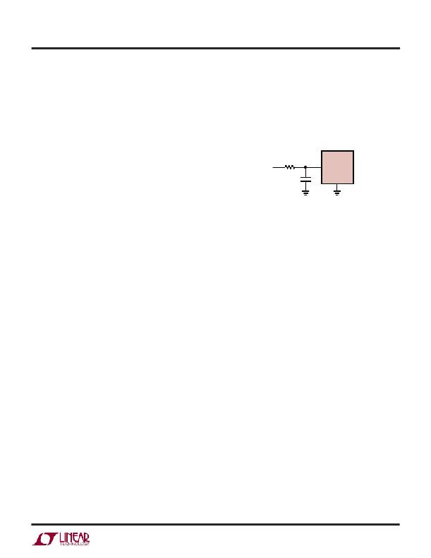
�pin� and� the� DAC� as� shown� in� Figure� 3.�
�Using� Ceramic� Input� and� Output� Capacitors�
�Higher� values,� lower� cost� ceramic� capacitors� are� now�
�becoming� available� in� smaller� case� sizes.� Their� high� ripple�
�current,� high� voltage� rating� and� low� ESR� make� them� ideal�
�for� switching� regulator� applications.� Because� the�
�DAC�
�10k�
�1000pF�
�LTC3408�
�REF�
�GND�
�3408� F03�
�LTC3408’s� control� loop� does� not� depend� on� the� output�
�capacitor’s� ESR� for� stable� operation,� ceramic� capacitors�
�can� be� used� freely� to� achieve� very� low� output� ripple� and�
�small� circuit� size.�
�However,� care� must� be� taken� when� ceramic� capacitors� are�
�used� at� the� input� and� the� output.� When� a� ceramic� capacitor�
�is� used� at� the� input� and� the� power� is� supplied� by� a� wall�
�adapter� through� long� wires,� a� load� step� at� the� output� can�
�induce� ringing� at� the� input,� V� IN� .� At� best,� this� ringing� can�
�couple� to� the� output� and� be� mistaken� as� loop� instability.� At�
�worst,� a� sudden� inrush� of� current� through� the� long� wires�
�can� potentially� cause� a� voltage� spike� at� V� IN� large� enough�
�to� damage� the� part.�
�When� choosing� the� input� and� output� ceramic� capacitors,�
�choose� the� X5R� or� X7R� dielectric� formulations.� These�
�dielectrics� have� the� best� temperature� and� voltage� charac-�
�teristics� of� all� the� ceramics� for� a� given� value� and� size.�
�Ceramic� capacitors� of� Y5V� material� are� not� recommended�
�because� normal� operating� voltages� cause� their� bulk� ca-�
�pacitance� to� become� much� less� than� the� nominal� value.�
�Programming� the� Output� Voltage� With� a� DAC�
�The� output� voltage� can� be� dynamically� programmed� to� any�
�voltage� from� 0.3V� to� 3.5V� with� an� external� DAC� driving� the�
�REF� pin.� When� the� output� is� commanded� low,� the� output�
�voltage� descends� quickly� in� forced� continuous� mode�
�pulling� current� from� the� output� and� transferring� it� to� the�
�input.� If� the� input� is� not� connected� to� a� low� impedance�
�source� capable� of� absorbing� the� energy,� the� input� voltage�
�could� rise� above� the� absolute� maximum� voltage� of� the� part�
�Figure� 3.� Filtering� the� REF� Pin�
�Efficiency� Considerations�
�The� efficiency� of� a� switching� regulator� is� equal� to� the�
�output� power� divided� by� the� input� power� times� 100%.� It� is�
�oftenusefultoanalyzeindividuallossestodeterminewhat�
�is� limiting� the� efficiency� and� which� change� would� produce�
�the� most� improvement.� Efficiency� can� be� expressed� as:�
�Efficiency� =� 100%� –� (L1� +� L2� +� L3� +� ...)�
�where� L1,� L2,� etc.� are� the� individual� losses� as� a� percentage�
�of� input� power.�
�Although� all� dissipative� elements� in� the� circuit� produce�
�losses,� two� main� sources� usually� account� for� most� of� the�
�losses� in� LTC3408� circuits:� V� IN� quiescent� current� and� I� 2� R�
�losses.� The� V� IN� quiescent� current� loss� dominates� the� effi-�
�ciency� loss� at� low� load� currents� whereas� the� I� 2� R� loss� domi-�
�nates� the� efficiency� loss� at� medium� to� high� load� currents.�
�In� a� typical� efficiency� plot,� the� efficiency� curve� at� low� load�
�currents can be misleading since the actual power lost is�
�of� little� consequence� as� illustrated� in� Figure� 4.�
�1.� The� V� IN� quiescent� current� consists� of� two� components:�
�the� DC� bias� current� as� given� in� the� electrical� characteris-�
�tics� and� the� internal� main� switch� and� synchronous� switch�
�gate� charge� currents.� The� gate� charge� current� results�
�from� switching� the� gate� capacitance� of� the� internal� power�
�MOSFET� switches.� Each� time� the� gate� is� switched� from�
�high� to� low� to� high� again,� a� packet� of� charge,� dQ,� moves�
�from� V� IN� to� ground.� The� resulting� dQ/dt� is� typically� larger�
�than� the� DC� bias� current.� In� continuous� mode,�
�3408f�
�9�
�相关PDF资料 |
PDF描述 |
|---|---|
| MIC2954-02WT | IC REG LDO 5V .25A TO-220-3 |
| MIC5239-2.5YMM | IC REG LDO 2.5V .5A 8-MSOP |
| 1812-473J | INDUCTOR UNSHIELDED 47UH SMD |
| LTC3408EDD | IC REG BUCK W/BYPASS TXRX 8-DFN |
| MIC5239-1.8YMM | IC REG LDO 1.8V .5A 8-MSOP |
相关代理商/技术参数 |
参数描述 |
|---|---|
| LTC3409 | 制造商:LINER 制造商全称:Linear Technology 功能描述:600mA Low Vin Buck Regulator in 3mm x 3mm DFN |
| LTC3409A | 制造商:LINER 制造商全称:Linear Technology 功能描述:600mA Low VIN Buck Regulator in 3mm × 3mm DFN |
| LTC3409AEDD | 制造商:LINER 制造商全称:Linear Technology 功能描述:600mA Low VIN Buck Regulator in 3mm × 3mm DFN |
| LTC3409AEDD#PBF | 功能描述:IC REG BUCK SYNC ADJ 0.6A 8DFN RoHS:是 类别:集成电路 (IC) >> PMIC - 稳压器 - DC DC 开关稳压器 系列:- 标准包装:2,500 系列:- 类型:升压(升压) 输出类型:可调式 输出数:1 输出电压:1.24 V ~ 30 V 输入电压:1.5 V ~ 12 V PWM 型:电流模式,混合 频率 - 开关:600kHz 电流 - 输出:500mA 同步整流器:无 工作温度:-40°C ~ 85°C 安装类型:表面贴装 封装/外壳:8-SOIC(0.154",3.90mm 宽) 包装:带卷 (TR) 供应商设备封装:8-SOIC |
| LTC3409AEDD#TRPBF | 功能描述:IC REG BUCK SYNC ADJ 0.6A 8DFN RoHS:是 类别:集成电路 (IC) >> PMIC - 稳压器 - DC DC 开关稳压器 系列:- 标准包装:2,500 系列:- 类型:升压(升压) 输出类型:可调式 输出数:1 输出电压:1.24 V ~ 30 V 输入电压:1.5 V ~ 12 V PWM 型:电流模式,混合 频率 - 开关:600kHz 电流 - 输出:500mA 同步整流器:无 工作温度:-40°C ~ 85°C 安装类型:表面贴装 封装/外壳:8-SOIC(0.154",3.90mm 宽) 包装:带卷 (TR) 供应商设备封装:8-SOIC |
发布紧急采购,3分钟左右您将得到回复。