- 您现在的位置:买卖IC网 > PDF目录14013 > LTC3523EUD-2#PBF (Linear Technology)IC REG BUCK BOOST SYNC ADJ 16QFN PDF资料下载
参数资料
| 型号: | LTC3523EUD-2#PBF |
| 厂商: | Linear Technology |
| 文件页数: | 9/16页 |
| 文件大小: | 0K |
| 描述: | IC REG BUCK BOOST SYNC ADJ 16QFN |
| 标准包装: | 121 |
| 类型: | 降压(降压),升压(升压) |
| 输出类型: | 可调式 |
| 输出数: | 2 |
| 输出电压: | 0.62 V ~ 5.5 V |
| 输入电压: | 1.8 V ~ 5.5 V |
| PWM 型: | 电流模式,混合 |
| 频率 - 开关: | 2.4MHz |
| 电流 - 输出: | 400mA,600mA |
| 同步整流器: | 是 |
| 工作温度: | -40°C ~ 85°C |
| 安装类型: | 表面贴装 |
| 封装/外壳: | 16-WFQFN 裸露焊盘 |
| 包装: | 管件 |
| 供应商设备封装: | 16-QFN-EP(3x3) |
�� �
�
�LTC3523/LTC3523-2�
�OPERATION�
�Step-Up� Anti-Ringing� Control�
�The� anti-ring� circuitry� connects� a� resistor� across� the� in-�
�ductor� to� prevent� high� frequency� ringing� on� the� SW1� pin�
�during� discontinuous� current� mode� operation.� The� ringing�
�of� the� resonant� circuit� formed� by� L� and� C� SW� (capacitance�
�on� SW� pin)� is� low� energy,� but� can� cause� EMI� radiation.�
�Step-Up� Output� Disconnect�
�The� LTC3523/LTC3523-2� step-up� is� designed� to� provide�
�true� output� disconnect� by� eliminating� body� diode� conduc-�
�tion� of� the� internal� P-channel� MOSFET� recti?er.� This� allows�
�for� V� OUT� to� go� to� zero� volts� during� shutdown,� drawing� no�
�current� from� the� input� source.� Controlling� the� P-channel�
�APPLICATIONS� INFORMATION�
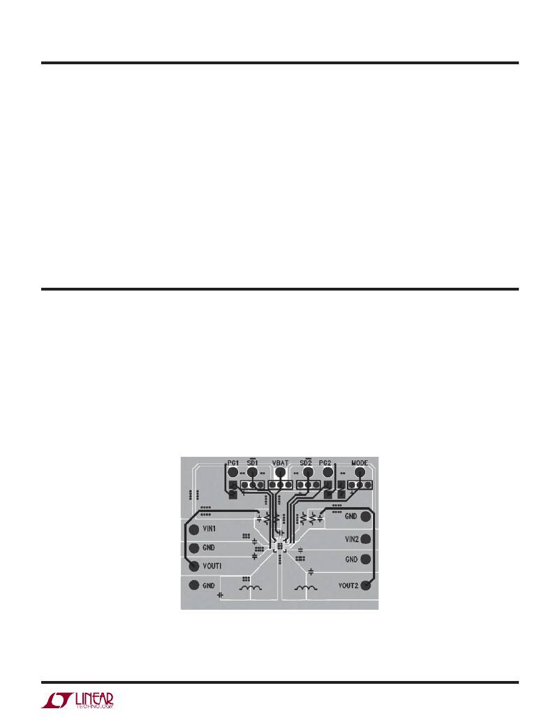
�PCB� LAYOUT� GUIDELINES�
�The� high� speed� operation� of� the� LTC3523/LTC3523-2�
�demands� careful� attention� to� board� layout.� You� will� not�
�get� advertised� performance� with� careless� layout.� Figure� 1�
�shows� the� recommended� component� placement.� A� large�
�ground� pin� copper� area� will� help� to� lower� the� chip� tem-�
�perature.� A� multilayer� board� with� a� separate� ground� plane�
�is� ideal,� but� not� absolutely� necessary.�
�MOSFET� body� diode� also� enables� inrush� current� limiting�
�at� turn-on,� minimizing� surge� currents� seen� by� the� input�
�supply.� Note� that� to� obtain� the� advantages� of� output� dis-�
�connect,� an� external� Schottky� diode� cannot� be� connected�
�between� SW1� and� V� OUT� .�
�Thermal� Shutdown�
�If� the� die� temperature� reaches� 160°C,� the� part� will� go� into�
�thermal� shutdown.� All� switches� will� be� turned� off� and�
�the� soft-start� capacitor� will� be� discharged.� The� device�
�will� be� enabled� again� when� the� die� temperature� drops� by�
�approximately� 15°C.�
�COMPONENT� SELECTION�
�Inductor� Selection�
�The� LTC3523/LTC3523-2� can� utilize� small� surface� mount�
�and� chip� inductors� due� to� its� fast� 1.2MHz� switching�
�frequency� and� for� the� 2.4MHz� version,� the� values� are�
�halved.� The� Inductor� current� ripple� is� typically� set� for�
�20%� to� 40%� of� the� peak� inductor� current� (I� P� ).� High�
�Figure� 1.� Recommended� Component� Placement� for� Double� Layer� Board�
�3523fb�
�9�
�相关PDF资料 |
PDF描述 |
|---|---|
| V28C24C100BG2 | CONVERTER MOD DC/DC 24V 100W |
| LTC3527EUD-1#PBF | IC REG BOOST SYNC ADJ DL 16QFN |
| V28C24C100BF3 | CONVERTER MOD DC/DC 24V 100W |
| LTC3527EUD#PBF | IC REG BOOST SYNC ADJ DL 16QFN |
| MAX6717AUKZWD6+T | IC SUPERVISOR MPU SOT23-5 |
相关代理商/技术参数 |
参数描述 |
|---|---|
| LTC3523EUD-2-TRPBF | 制造商:LINER 制造商全称:Linear Technology 功能描述:Synchronous 600mA Step-Up and 400mA Step-Down DC/DC Converters |
| LTC3523EUD-PBF | 制造商:LINER 制造商全称:Linear Technology 功能描述:Synchronous 600mA Step-Up and 400mA Step-Down DC/DC Converters |
| LTC3523EUD-TRPBF | 制造商:LINER 制造商全称:Linear Technology 功能描述:Synchronous 600mA Step-Up and 400mA Step-Down DC/DC Converters |
| LTC3524 | 制造商:LINER 制造商全称:Linear Technology 功能描述:Adjustable TFT Bias Supply with WLED Driver |
| LTC3524EUF | 制造商:LINER 制造商全称:Linear Technology 功能描述:Adjustable TFT Bias Supply with WLED Driver |
发布紧急采购,3分钟左右您将得到回复。