- 您现在的位置:买卖IC网 > PDF目录1830 > LTC3544BEUD#TRPBF (Linear Technology)IC REG BUCK SYNC ADJ QUAD 16QFN PDF资料下载
参数资料
| 型号: | LTC3544BEUD#TRPBF |
| 厂商: | Linear Technology |
| 文件页数: | 11/18页 |
| 文件大小: | 0K |
| 描述: | IC REG BUCK SYNC ADJ QUAD 16QFN |
| 标准包装: | 2,500 |
| 类型: | 降压(降压) |
| 输出类型: | 可调式 |
| 输出数: | 4 |
| 输出电压: | 0.8 V ~ 5.5 V |
| 输入电压: | 2.25 V ~ 5.5 V |
| PWM 型: | 电流模式 |
| 频率 - 开关: | 2.25MHz |
| 电流 - 输出: | 100mA,200mA(2),300mA |
| 同步整流器: | 是 |
| 工作温度: | -40°C ~ 85°C |
| 安装类型: | 表面贴装 |
| 封装/外壳: | 16-WFQFN 裸露焊盘 |
| 包装: | 带卷 (TR) |
| 供应商设备封装: | 16-QFN-EP(3x3) |
�� �
�
�LTC3544B�
�APPLICATIONS� INFORMATION�
�Δ� V� OUT�
�?� Δ� I� L� ?� ESR� +�
�generally far exceeds the I� RIPPLE(P-P)� requirement. The�
�output� ripple� Δ� V� OUT� is� determined� by:�
�?� 1� ?�
�?�
�?� 8?� ?� ?� C� OUT� ?�
�LTC3544B�
�V� FB�
�0.8V� ≤� V� OUT� ≤� 5.5V�
�R2�
�R1�
�C� F�
�V� OUT� =� 0� .� 8� V� ?� 1� +�
�wheref=operatingfrequency,C� OUT� =outputcapacitance�
�and� Δ� I� L� =� ripple� current� in� the� inductor.� For� a� fixed� output�
�voltage,� the� output� ripple� is� highest� at� maximum� input�
�voltage� since� Δ� I� L� increases� with� input� voltage.�
�Using� Ceramic� Input� and� Output� Capacitors�
�Higher� value,� lower� cost,� ceramic� capacitors� are� now�
�widely� available� in� smaller� case� sizes.� Their� high� ripple�
�current,� high� voltage� rating� and� low� ESR� make� them�
�ideal� for� switching� regulator� applications.� Because� the�
�LTC3544B’s� control� loop� does� not� depend� on� the� output�
�capacitor’s� ESR� for� stable� operation,� ceramic� capacitors�
�can� be� used� freely� to� achieve� very� low� output� ripple� and�
�small� circuit� size.�
�However,� care� must� be� taken� when� ceramic� capacitors� are�
�used� at� the� input� and� the� output.� When� a� ceramic� capacitor�
�is� used� at� the� input� and� the� power� is� supplied� by� a� wall�
�adapter� through� long� wires,� a� load� step� at� the� output� can�
�induce� ringing� at� the� input,� V� IN� .� At� best,� this� ringing� can�
�couple� to� the� output� and� be� mistaken� as� loop� instability.� At�
�worst,� a� sudden� inrush� of� current� through� the� long� wires�
�can� potentially� cause� a� voltage� spike� at� V� IN� ,� large� enough�
�to� damage� the� part.�
�When� choosing� the� input� and� output� ceramic� capacitors,�
�choose� the� X5R� or� X7R� dielectric� formulations.� These�
�dielectrics� have� the� best� temperature� and� voltage� charac-�
�teristics� of� all� the� ceramics� for� a� given� value� and� size.�
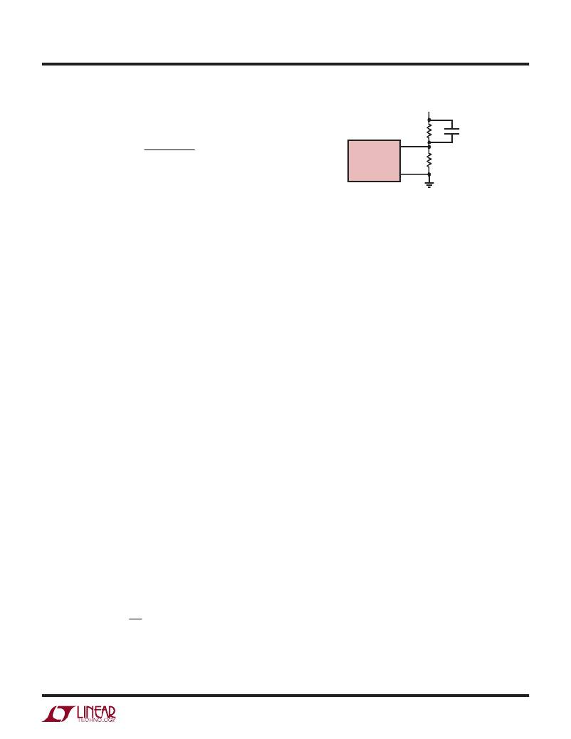
�Output� Voltage� Programming�
�The� output� voltage� is� set� by� tying� V� FB� to� a� resistive� divider�
�according� to� the� following� formula:�
�?� R2� ?�
�?�
�?� R� 1� ?�
�The� external� resistive� divider� is� connected� to� the� output�
�allowing� remote� voltage� sensing� as� shown� in� Figure� 2.�
�GND�
�3544B� F02�
�Figure� 2.� Setting� the� LTC3544B� Output� Voltage�
�Keeping� the� current� in� the� resistors� small� maximizes� the�
�efficiency,� but� making� them� too� small� may� allow� stray�
�capacitance� to� cause� noise� problems� or� reduce� the� phase�
�margin� of� the� control� loop.� It� is� recommended� that� the�
�total� feedback� resistor� string� be� kept� to� under� 100k.�
�To� improve� the� frequency� response� of� the� control� loop,� a�
�feed� forward� capacitor,� C� F� ,� may� be� used.� Great� care� should�
�be� taken� to� route� the� feedback� line� away� from� noise� sources�
�such� as� the� inductor� of� the� SW� line.�
�Efficiency� Considerations�
�The� efficiency� of� a� switching� regulator� is� equal� to� the� output�
�power� divided� by� the� input� power� times� 100%.� It� is� often�
�useful� to� analyze� individual� losses� to� determine� what� is�
�limiting� the� efficiency� and� which� change� would� produce�
�the� most� improvement.� Efficiency� can� be� expressed� as:�
�Efficiency� =� 100%� –� (L1� +� L2� +� L3� +� ...)� where� L1,� L2,� etc.�
�are� the� individual� losses� as� a� percentage� of� input� power.�
�Although� all� dissipative� elements� in� the� circuit� produce�
�losses,� two� main� sources� usually� account� for� most� of� the�
�losses� in� LTC3544B� circuits:� V� IN� quiescent� current� and� I� 2� R�
�losses.� V� IN� quiescent� current� loss� dominates� the� efficiency�
�loss� at� low� load� currents,� whereas� the� I� 2� R� loss� dominates�
�the� efficiency� loss� at� medium� to� high� load� currents.�
�1.� The� quiescent� current� is� due� to� two� components:� the�
�DC� bias� current� as� given� in� the� electrical� characteristics�
�and� the� internal� main� switch� and� synchronous� switch�
�gate� charge� currents.� The� gate� charge� current� results�
�from� switching� the� gate� capacitance� of� the� internal� power�
�MOSFET� switches.� Each� time� the� gate� is� switched� from�
�high� to� low� to� high� again,� a� packet� of� charge,� dQ,� moves�
�from� PV� IN� to� ground.� The� resulting� dQ/dt� is� the� current� out�
�of� PV� IN� that� is� typically� larger� than� the� DC� bias� current� and�
�3544bfb�
� �
�相关PDF资料 |
PDF描述 |
|---|---|
| LTC3545IUD-1#TRPBF | IC REG BUCK SYNC ADJ 0.8A 16QFN |
| LTC3546IFE#TRPBF | IC REG BUCK SYNC ADJ DL 28TSSOP |
| LTC3547EDDB-1#TRPBF | IC REG BUCK SYNC ADJ .3A DL 8DFN |
| LTC3548IMSE#TRPBF | IC REG BUCK SYNC ADJ DL 10MSOP |
| LTC3549EDCB#TRPBF | IC REG BUCK SYNC ADJ 0.25A 6DFN |
相关代理商/技术参数 |
参数描述 |
|---|---|
| LTC3544EUD | 制造商:LINER 制造商全称:Linear Technology 功能描述:Quad Synchronous Step-Down Regulator: 2.25MHz, 300mA, 200mA, 200mA, 100mA |
| LTC3544EUD#PBF | 功能描述:IC REG BUCK SYNC ADJ QUAD 16QFN RoHS:是 类别:集成电路 (IC) >> PMIC - 稳压器 - DC DC 开关稳压器 系列:- 标准包装:250 系列:- 类型:降压(降压) 输出类型:固定 输出数:1 输出电压:1.2V 输入电压:2.05 V ~ 6 V PWM 型:电压模式 频率 - 开关:2MHz 电流 - 输出:500mA 同步整流器:是 工作温度:-40°C ~ 85°C 安装类型:表面贴装 封装/外壳:6-UFDFN 包装:带卷 (TR) 供应商设备封装:6-SON(1.45x1) 产品目录页面:1032 (CN2011-ZH PDF) 其它名称:296-25628-2 |
| LTC3544EUD#TRPBF | 功能描述:IC REG BUCK SYNC ADJ QUAD 16QFN RoHS:是 类别:集成电路 (IC) >> PMIC - 稳压器 - DC DC 开关稳压器 系列:- 标准包装:2,500 系列:- 类型:降压(降压) 输出类型:固定 输出数:1 输出电压:1.2V,1.5V,1.8V,2.5V 输入电压:2.7 V ~ 20 V PWM 型:- 频率 - 开关:- 电流 - 输出:50mA 同步整流器:是 工作温度:-40°C ~ 125°C 安装类型:表面贴装 封装/外壳:10-TFSOP,10-MSOP(0.118",3.00mm 宽)裸露焊盘 包装:带卷 (TR) 供应商设备封装:10-MSOP 裸露焊盘 |
| LTC3544EUDPBF | 制造商:Linear Technology 功能描述:2.25MHz Sync Step-Down Converter LTC3544 |
| LTC3544EUD-PBF | 制造商:LINER 制造商全称:Linear Technology 功能描述:Quad Synchronous Step-Down Regulator: 2.25MHz, 300mA, 200mA, 200mA, 100mA |
发布紧急采购,3分钟左右您将得到回复。