- 您现在的位置:买卖IC网 > PDF目录30770 > LTC3546EFE (LINEAR TECHNOLOGY CORP) DUAL SWITCHING CONTROLLER, 4000 kHz SWITCHING FREQ-MAX, PDSO28 PDF资料下载
参数资料
| 型号: | LTC3546EFE |
| 厂商: | LINEAR TECHNOLOGY CORP |
| 元件分类: | 稳压器 |
| 英文描述: | DUAL SWITCHING CONTROLLER, 4000 kHz SWITCHING FREQ-MAX, PDSO28 |
| 封装: | 4.40 MM, PLASTIC, TSSOP-28 |
| 文件页数: | 13/28页 |
| 文件大小: | 356K |
| 代理商: | LTC3546EFE |
第1页第2页第3页第4页第5页第6页第7页第8页第9页第10页第11页第12页当前第13页第14页第15页第16页第17页第18页第19页第20页第21页第22页第23页第24页第25页第26页第27页第28页
LTC3546
20
3546fb
APPLICATIONS INFORMATION
tors. This mode provides the best low current efciency at
thecostofahigheroutputvoltageripple.WhenSYNC/MODE
isconnectedtoground,pulse-skippingoperationisselected
for both regulators. This mode provides a lower output volt-
age and current ripple at the cost of low current efciency.
Applying VIN/2 results in forced continuous mode for both
regulators. This mode creates a xed output ripple and is
capable of sinking some current (about 1/2 ΔIL). Since
the switching noise is constant in this mode, it is also the
easiest to lter out. During initial start-up, pulse-skipping
mode is forced until the PGOOD pin goes high.
The LTC3546 can also be synchronized to an external
clock signal by the SYNC/MODE pin. An internal phase
locked loop locks to the incoming signal to provide for
180° out-of-phase operation as well as correct slope
compensation. With external synchronization the FREQ
pin is used for externally compensating the internal phase
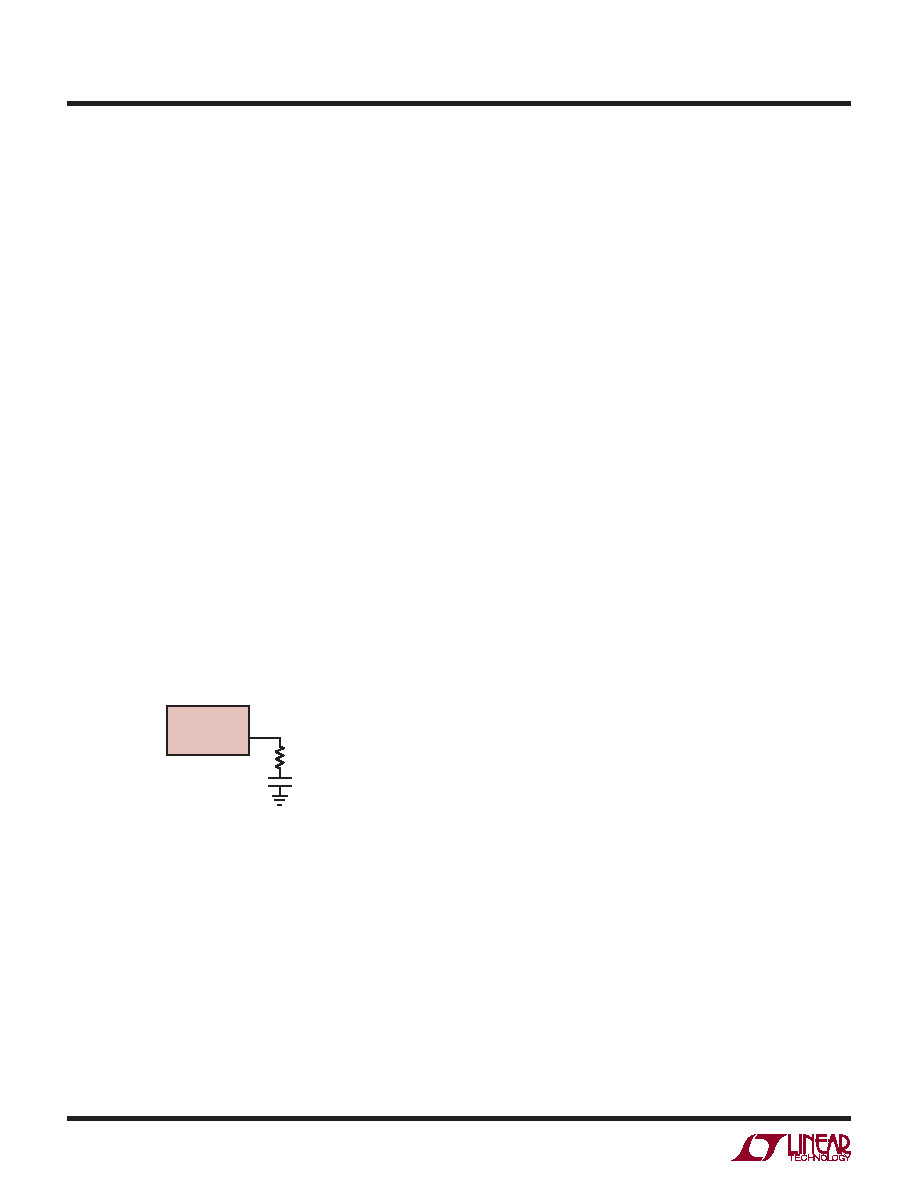
locked loop. Typical values used for compensation are 200k
and 100pf, as shown in Figure 6. During synchronization,
the regulator operating mode is forced to pulse skipping.
The P-channel switch turn on is synchronized to the rising
edge of the external clock.
When using an external clock, with the PHASE pin low, the
switching of the two channels occur 180° out-of-phase.
estimated using the percentage of overshoot seen at this
pin, or by examining the rise time at this pin.
The ITH external components shown in the Figure 9 circuit
will provide an adequate starting point for most applica-
tions. The series R-C lter sets the dominant pole-zero
loop compensation. The values can be modied slightly
(from 0.5 to 2 times their suggested values) to optimize
transient response once the nal PC layout is done and
the particular output capacitor type and value have been
determined. The output capacitors need to be selected
because of various types and values determine the loop
feedback factor gain and phase. An output current pulse
of 20% to 100% of full load current having a rise time
of 1μs to 10μs will produce output voltage and ITH pin
waveforms that will give a sense of overall loop stability
without breaking the feedback loop.
Switching regulators take several cycles to respond to
a step in load current. When a load step occurs, VOUT
immediately shifts by an amount equal to ΔILOAD ESR,
where ESR is the effective series resistance of COUT. The
ΔILOAD also begins to charge or discharge COUT generat-
ing a feedback error signal used by the regulator to return
VOUT to its steady-state value. During this recovery time,
VOUT can be monitored for overshoot or ringing that would
indicate a stability problem.
The initial output voltage step may not be within the band-
width of the feedback loop, so the standard second order
overshoot/DC ratio cannot be used to determine phase
margin. The gain of the loop increases with RITH and the
bandwidth of the loop increases with decreasing CITH. If
RITH is increased by the same factor that CITH is decreased,
the zero frequency will be kept the same, thereby keeping
the phase the same in the most critical frequency range
of the feedback loop. In addition, feedforward capacitors,
CFF1 and CFF2, can be added to improve the high frequency
response, as shown in Figure 9. Capacitor CFF1 provides
phase lead by creating a high frequency zero with R1
which improves the phase margin for the 1A SW1 chan-
nel. Capacitor CFF2 provides phase lead by creating a high
frequency zero with R3 which improves the phase margin
for the 3A SW1D/SW2 channel.
The output voltage settling behavior is related to the stability
of the closed-loop system and will demonstrate the actual
Figure 6. PLL Compensation
3546 F06
LTC3546
200k
FREQ
100pF
Checking Transient Response
The ITH pin compensation allows the transient response
to be optimized for a wide range of loads and output
capacitors. The availability of the ITH pin not only allows
optimization of the control loop behavior but also pro-
vides a DC-coupled and AC ltered closed loop response
test point. The DC step, rise time and settling at this test
point truly reects the closed loop response. Assuming a
predominantly second order system, phase margin and/or
damping factor can be estimated using the percentage of
overshoot seen at this pin. The bandwidth can also be
相关PDF资料 |
PDF描述 |
|---|---|
| LTC3546IFE#TRPBF | DUAL SWITCHING CONTROLLER, 4000 kHz SWITCHING FREQ-MAX, PDSO28 |
| LTC3546IFE#TR | DUAL SWITCHING CONTROLLER, 4000 kHz SWITCHING FREQ-MAX, PDSO28 |
| LTC3554EUD-2#TRPBF | 0.6 A BATTERY CHARGE CONTROLLER, 2590 kHz SWITCHING FREQ-MAX, PQCC20 |
| LTC3554EUD#PBF | 0.6 A BATTERY CHARGE CONTROLLER, 2590 kHz SWITCHING FREQ-MAX, PQCC20 |
| LTC3565EDD#PBF | 2.5 A SWITCHING REGULATOR, 4000 kHz SWITCHING FREQ-MAX, PDSO10 |
相关代理商/技术参数 |
参数描述 |
|---|---|
| LTC3546EFE#PBF | 功能描述:IC REG BUCK SYNC ADJ DL 28TSSOP RoHS:是 类别:集成电路 (IC) >> PMIC - 稳压器 - DC DC 开关稳压器 系列:- 标准包装:250 系列:- 类型:降压(降压) 输出类型:固定 输出数:1 输出电压:1.2V 输入电压:2.05 V ~ 6 V PWM 型:电压模式 频率 - 开关:2MHz 电流 - 输出:500mA 同步整流器:是 工作温度:-40°C ~ 85°C 安装类型:表面贴装 封装/外壳:6-UFDFN 包装:带卷 (TR) 供应商设备封装:6-SON(1.45x1) 产品目录页面:1032 (CN2011-ZH PDF) 其它名称:296-25628-2 |
| LTC3546EFE#PBF | 制造商:Linear Technology 功能描述:IC DUAL SYNC STEP-DOWN DC/DC REG 28-TSSO |
| LTC3546EFE#TRPBF | 功能描述:IC REG BUCK SYNC ADJ DL 28TSSOP RoHS:是 类别:集成电路 (IC) >> PMIC - 稳压器 - DC DC 开关稳压器 系列:- 设计资源:Design Support Tool 标准包装:1 系列:- 类型:升压(升压) 输出类型:固定 输出数:1 输出电压:3V 输入电压:0.75 V ~ 2 V PWM 型:- 频率 - 开关:- 电流 - 输出:100mA 同步整流器:是 工作温度:-40°C ~ 85°C 安装类型:表面贴装 封装/外壳:SOT-23-5 细型,TSOT-23-5 包装:剪切带 (CT) 供应商设备封装:TSOT-23-5 其它名称:AS1323-BTTT-30CT |
| LTC3546EFEPBF | 制造商:LINER 制造商全称:Linear Technology 功能描述:Dual Synchronous, 3A/1A or 2A/2A Confi gurable Step-Down DC/DC Regulator |
| LTC3546EFETRPBF | 制造商:LINER 制造商全称:Linear Technology 功能描述:Dual Synchronous, 3A/1A or 2A/2A Confi gurable Step-Down DC/DC Regulator |
发布紧急采购,3分钟左右您将得到回复。