- 您现在的位置:买卖IC网 > PDF目录79697 > LTC3565IDD#TRPBF (LINEAR TECHNOLOGY CORP) 2.5 A SWITCHING REGULATOR, 4000 kHz SWITCHING FREQ-MAX, PDSO10 PDF资料下载
参数资料
| 型号: | LTC3565IDD#TRPBF |
| 厂商: | LINEAR TECHNOLOGY CORP |
| 元件分类: | 稳压器 |
| 英文描述: | 2.5 A SWITCHING REGULATOR, 4000 kHz SWITCHING FREQ-MAX, PDSO10 |
| 封装: | 3 X 3 MM, LEAD FREE, PLASTIC, MO-229WEED-2, DFN-10 |
| 文件页数: | 21/22页 |
| 文件大小: | 587K |
| 代理商: | LTC3565IDD#TRPBF |
LTC3565
3565fa
RT (Pin 1): Timing Resistor Pin. The oscillator frequency
is programmed by connecting a resistor from this pin to
ground.
RUN (Pin 2): Converter Enable Pin. Forcing this pin above
1.5V enables this part, while forcing it below 0.3V causes
the device to shut down. In shutdown, the device draws
<1A supply current. This pin must be driven; do not float.
SYNC/MODE (Pin 3): Combination Mode Selection and
Oscillator Synchronization Pin. This pin controls the
operation of the device. When tied to SVIN or GND, Burst
Mode operation or pulse skipping mode is selected,
respectively. If this pin is held at half of SVIN, the forced
continuous mode is selected. The oscillation frequency
can be synchronized to an external oscillator applied to
this pin. When synchronized to an external clock, pulse
skip mode is selected.
SW (Pin 4): The Switch Node Connection to the Inductor.
This pin swings from PVIN to GND.
pin Functions
GND (Pin 5, Exposed Pad Pin 11): Main Power Ground
Pin. Connect to the (–) terminal of COUT, and (–) terminal
of CIN. The exposed pad must be soldered to electrical
ground on PCB ground.
PVIN (Pin 6): Main Supply Pin. Must be closely decoupled
to GND.
SVIN (Pin 7): The Signal Power Pin. All active circuitry is
powered from this pin. Must be closely decoupled to GND.
SVIN must be greater than or equal to PVIN.
PGOOD (Pin 8): The Power Good Pin. This common drain
logic output is pulled to GND when the output voltage is
not within ±7% of regulation.
VFB (Pin 9): Receives the feedback voltage from the ex-
ternal resistive divider across the output. Nominal voltage
for this pin is 0.6V.
ITH (Pin 10): Error Amplifier Compensation Point. The
current comparator threshold increases with this control
voltage. Nominal voltage range for this pin is 0.4V to
1.4V.
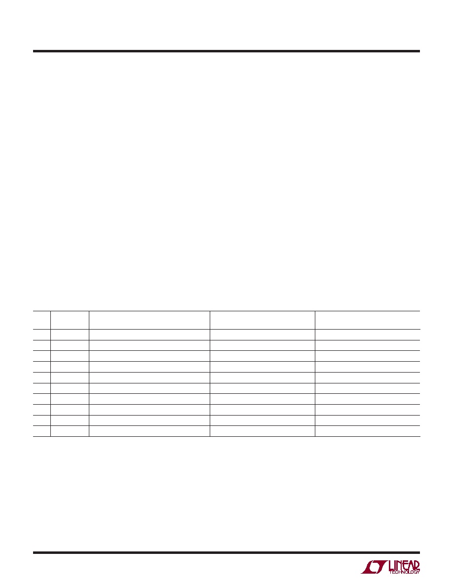
NOMINAL (V)
ABSOLUTE MAX (V)
PIN
NAME
DESCRIPTION
MIN
TYP
MAX
MIN
MAX
1
RT
Timing Resistor
–0.3
0.4
SVIN
–0.3
SVIN + 0.3
2
RUN
Enable Pin
–0.3
SVIN
–0.3
SVIN
3
SYNC/MODE Mode Select/Synchronization Pin
0
SVIN
–0.3
SVIN + 0.3
4
SW
Switch Node
0
PVIN
–0.3
PVIN + 0.3
5
GND
Main Power Ground
0
6
PVIN
Main Power Supply
–0.3
5.5
–0.3
6
7
SVIN
Signal Power Supply
2.5
5.5
–0.3
6
8
PGOOD
Power Good Pin
0
SVIN
–0.3
SVIN + 0.3
9
VFB
Output Feedback Pin
0
0.8
1.0
–0.3
SVIN + 0.3
10
ITH
Error Amplifier Compensation
0
1.5
–0.3
SVIN + 0.3
相关PDF资料 |
PDF描述 |
|---|---|
| LS75-12 | 1-OUTPUT DC-DC UNREG PWR SUPPLY MODULE |
| LED15-48S05W | 1-OUTPUT 15 W DC-DC REG PWR SUPPLY MODULE |
| LFFSWG-TTL-70F | SQUARE, 0.07 MHz, WAVEFORM GENERATION, PDIP4 |
| LFFSWG-TTL-55J | SQUARE, 0.055 MHz, WAVEFORM GENERATION, PDSO4 |
| LH2540-2-V3 | 2-OUTPUT 51 W AC-DC REG PWR SUPPLY MODULE |
相关代理商/技术参数 |
参数描述 |
|---|---|
| LTC3565IMSE | 制造商:LINER 制造商全称:Linear Technology 功能描述:1.25A, 4MHz, Synchronous Step-Down DC/DC Converter |
| LTC3565IMSE#PBF | 功能描述:IC REG BUCK SYNC ADJ 10MSOP RoHS:是 类别:集成电路 (IC) >> PMIC - 稳压器 - DC DC 开关稳压器 系列:- 标准包装:2,500 系列:- 类型:升压(升压) 输出类型:可调式 输出数:1 输出电压:1.24 V ~ 30 V 输入电压:1.5 V ~ 12 V PWM 型:电流模式,混合 频率 - 开关:600kHz 电流 - 输出:500mA 同步整流器:无 工作温度:-40°C ~ 85°C 安装类型:表面贴装 封装/外壳:8-SOIC(0.154",3.90mm 宽) 包装:带卷 (TR) 供应商设备封装:8-SOIC |
| LTC3565IMSE#TRPBF | 功能描述:IC REG BUCK SYNC ADJ 10MSOP RoHS:是 类别:集成电路 (IC) >> PMIC - 稳压器 - DC DC 开关稳压器 系列:- 标准包装:2,500 系列:- 类型:升压(升压) 输出类型:可调式 输出数:1 输出电压:1.24 V ~ 30 V 输入电压:1.5 V ~ 12 V PWM 型:电流模式,混合 频率 - 开关:600kHz 电流 - 输出:500mA 同步整流器:无 工作温度:-40°C ~ 85°C 安装类型:表面贴装 封装/外壳:8-SOIC(0.154",3.90mm 宽) 包装:带卷 (TR) 供应商设备封装:8-SOIC |
| LTC3565IMSEPBF | 制造商:LINER 制造商全称:Linear Technology 功能描述:1.25A, 4MHz, Synchronous Step-Down DC/DC Converter |
| LTC3565IMSE-PBF | 制造商:LINER 制造商全称:Linear Technology 功能描述:1.25A, 4MHz, Synchronous Step-Down DC/DC Converter |
发布紧急采购,3分钟左右您将得到回复。