- 您现在的位置:买卖IC网 > PDF目录80091 > LTC3568IDD#PBF (LINEAR TECHNOLOGY CORP) 4 A SWITCHING REGULATOR, 4000 kHz SWITCHING FREQ-MAX, PDSO10 PDF资料下载
参数资料
| 型号: | LTC3568IDD#PBF |
| 厂商: | LINEAR TECHNOLOGY CORP |
| 元件分类: | 稳压器 |
| 英文描述: | 4 A SWITCHING REGULATOR, 4000 kHz SWITCHING FREQ-MAX, PDSO10 |
| 封装: | 3 X 3 MM, LEAD FREE, PLASTIC, MO-229WEED-2, DFN-10 |
| 文件页数: | 15/18页 |
| 文件大小: | 300K |
| 代理商: | LTC3568IDD#PBF |
LTC3568
3568fa
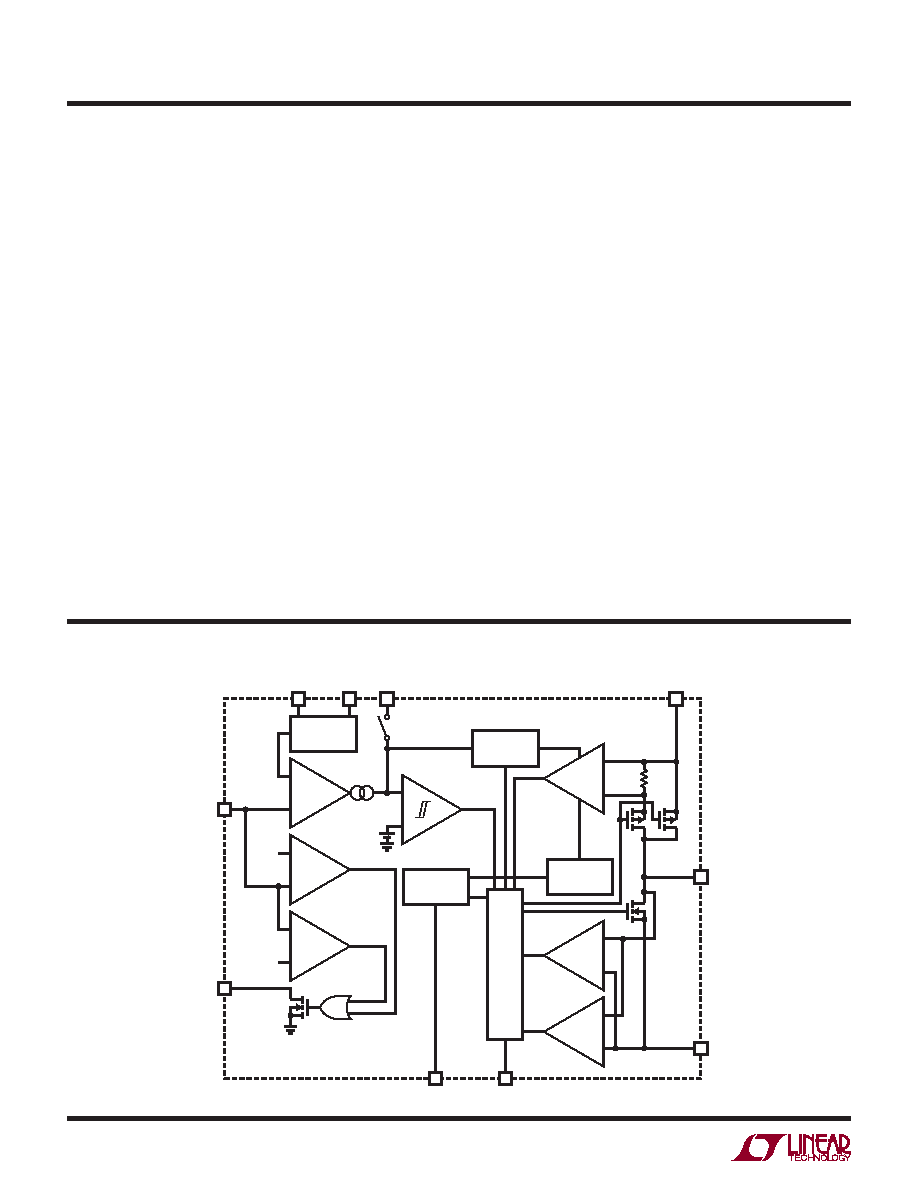
pin FuncTions
SHDN/RT (Pin 1): Combination Shutdown and Timing
Resistor Pin. The oscillator frequency is programmed by
connecting a resistor from this pin to ground. Forcing
this pin to SVIN causes the device to be shut down. In
shutdown all functions are disabled.
SYNC/MODE(Pin2): Combination Mode Selection and
Oscillator Synchronization Pin. This pin controls the op-
eration of the device. When tied to SVIN or SGND, Burst
Mode operation or pulse skipping mode is selected,
respectively. If this pin is held at half of SVIN, the forced
continuous mode is selected. The oscillation frequency
can be syncronized to an external oscillator applied to
this pin. When synchronized to an external clock pulse
skip mode is selected.
SGND (Pin 3): The Signal Ground Pin. All small signal
componentsandcompensationcomponentsshouldbecon-
nected to this ground (see Board Layout Considerations).
SW(Pin4): The Switch Node Connection to the Inductor.
This pin swings from PVIN to PGND.
PGND(Pin5): Main Power Ground Pin. Connect to the
(–) terminal of COUT, and (–) terminal of CIN.
PVIN(Pin6): Main Supply Pin. Must be closely decoupled
to PGND.
SVIN(Pin7): The Signal Power Pin. All active circuitry
is powered from this pin. Must be closely decoupled to
SGND. SVIN must be greater than or equal to PVIN.
PGOOD(Pin8): The Power Good Pin. This common drain
logic output is pulled to SGND when the output voltage is
not within ±7.5% of regulation.
VFB(Pin9): Receives the feedback voltage from the ex-
ternal resistive divider across the output. Nominal voltage
for this pin is 0.8V.
ITH(Pin10): Error Amplifier Compensation Point. The
current comparator threshold increases with this control
voltage. Nominal voltage range for this pin is 0V to 1.5V.
GND (Exposed Pad Pin 11): Thermal Ground. Con-
nect to SGND and solder to the PCB for rated thermal
performance.
block DiagraM
–
+
8
9
–
+
–
+
0.74V
0.8V
ERROR
AMPLIFIER
VB
BURST
COMPARATOR
HYSTERESIS = 80mV
BCLAMP
NMOS
COMPARATOR
PMOS CURRENT
COMPARATOR
REVERSE
COMPARATOR
0.86V
5
SW
4
PGOOD
10
ITH
VFB
1
SHDN/RT
2
SYNC/MODE
3568 BD
6
PVIN
3
SGND
7
SVIN
SLOPE
COMPENSATION
VOLTAGE
REFERENCE
OSCILLATOR
LOGIC
ITH
LIMIT
–
+
–
+
–
PGND
相关PDF资料 |
PDF描述 |
|---|---|
| LES015YH21N | 1-OUTPUT 15 W DC-DC REG PWR SUPPLY MODULE |
| LES015YJ18N | 1-OUTPUT 15 W DC-DC REG PWR SUPPLY MODULE |
| LES015YJ4N | 1-OUTPUT 15 W DC-DC REG PWR SUPPLY MODULE |
| LES015ZG38N | 1-OUTPUT 15 W DC-DC REG PWR SUPPLY MODULE |
| LM2320-7ERD2HF | 2-OUTPUT 50 W AC-DC REG PWR SUPPLY MODULE |
相关代理商/技术参数 |
参数描述 |
|---|---|
| LTC3569 | 制造商:LINER 制造商全称:Linear Technology 功能描述:7-Channel Confi gurable High Power PMIC |
| LTC3569EFE | 制造商:Linear Technology 功能描述:DC/DC Converter Chip |
| LTC3569EFE#PBF | 功能描述:IC REG BUCK SYNC ADJ 16TSSOP RoHS:是 类别:集成电路 (IC) >> PMIC - 稳压器 - DC DC 开关稳压器 系列:- 标准包装:250 系列:- 类型:降压(降压) 输出类型:固定 输出数:1 输出电压:1.2V 输入电压:2.05 V ~ 6 V PWM 型:电压模式 频率 - 开关:2MHz 电流 - 输出:500mA 同步整流器:是 工作温度:-40°C ~ 85°C 安装类型:表面贴装 封装/外壳:6-UFDFN 包装:带卷 (TR) 供应商设备封装:6-SON(1.45x1) 产品目录页面:1032 (CN2011-ZH PDF) 其它名称:296-25628-2 |
| LTC3569EFE#TRPBF | 功能描述:IC REG BUCK SYNC ADJ 16TSSOP RoHS:是 类别:集成电路 (IC) >> PMIC - 稳压器 - DC DC 开关稳压器 系列:- 标准包装:2,500 系列:- 类型:降压(降压) 输出类型:固定 输出数:1 输出电压:1.2V,1.5V,1.8V,2.5V 输入电压:2.7 V ~ 20 V PWM 型:- 频率 - 开关:- 电流 - 输出:50mA 同步整流器:是 工作温度:-40°C ~ 125°C 安装类型:表面贴装 封装/外壳:10-TFSOP,10-MSOP(0.118",3.00mm 宽)裸露焊盘 包装:带卷 (TR) 供应商设备封装:10-MSOP 裸露焊盘 |
| LTC3569EFE-PBF | 制造商:LINER 制造商全称:Linear Technology 功能描述:Triple Buck Regulator With 1.2A and Two 600mA Outputs and Individual Programmable References |
发布紧急采购,3分钟左右您将得到回复。