- 您现在的位置:买卖IC网 > PDF目录80091 > LTC3568IDD#PBF (LINEAR TECHNOLOGY CORP) 4 A SWITCHING REGULATOR, 4000 kHz SWITCHING FREQ-MAX, PDSO10 PDF资料下载
参数资料
| 型号: | LTC3568IDD#PBF |
| 厂商: | LINEAR TECHNOLOGY CORP |
| 元件分类: | 稳压器 |
| 英文描述: | 4 A SWITCHING REGULATOR, 4000 kHz SWITCHING FREQ-MAX, PDSO10 |
| 封装: | 3 X 3 MM, LEAD FREE, PLASTIC, MO-229WEED-2, DFN-10 |
| 文件页数: | 6/18页 |
| 文件大小: | 300K |
| 代理商: | LTC3568IDD#PBF |
LTC3568
3568fa
applicaTions inForMaTion
DesignExample
Asadesignexample,considerusingtheLTC3568inatypical
application with VIN = 5V. The load requires a maximum
of 1.8A in active mode and 10mA in standby mode. The
output voltage is VOUT = 2.5V. Since the load still needs
power in standby, Burst Mode operation is selected for
good low load efficiency.
First, calculate the timing resistor:
R
MHz
k
T =
(
)
=
9 78 10 1
323 8
11
1 08
.
.
Use a standard value of 324k. Next, calculate the inductor
value for about 40% ripple current at maximum VIN:
L
V
MHz
mA
V
H
=
=
2 5
1
720
1
2 5
5
1 7
.
.
Choosing the closest inductor from a vendor of 2H,
results in a maximum ripple current of:
Δ =
=
I
V
MHz
V
mA
L
2 5
1
2
1
2 5
5
625
.
.
For cost reasons, a ceramic capacitor will be used. COUT
selection is then based on load step droop instead of ESR
requirements. For a 5% output droop:
C
A
MHz
V
F
OUT ≈
=
2 5
1 8
1
5
2 5
36
.
( % . )
The closest standard value is 22F plus 10F. Since the
supply’s output impedance is very low, CIN is typically a
22F. In noisy environments, decoupling SVIN from PVIN
with an R6/C8 filter of 1
Ω/0.1F may help, but is typically
not needed.
The output voltage can now be programmed by choosing
the values of R1 and R2. To maintain high efficiency, the
current in these resistors should be kept small. Choosing
2A with the 0.8V feedback voltage makes R1~400k. A
close standard 1% resistor is 412k and R2 is then 887k.
The compensation should be optimized for these compo-
nentsbyexaminingtheloadstepresponsebutagoodplace
to start for the LTC3568 is with a 13k
Ω and 1000pF filter.
The output capacitor may need to be increased depending
on the actual undershoot during a load step.
The PGOOD pin is a common drain output and requires
a pull-up resistor. A 100k resistor is used for adequate
speed.
Figure 1 shows the complete schematic for this design
example.
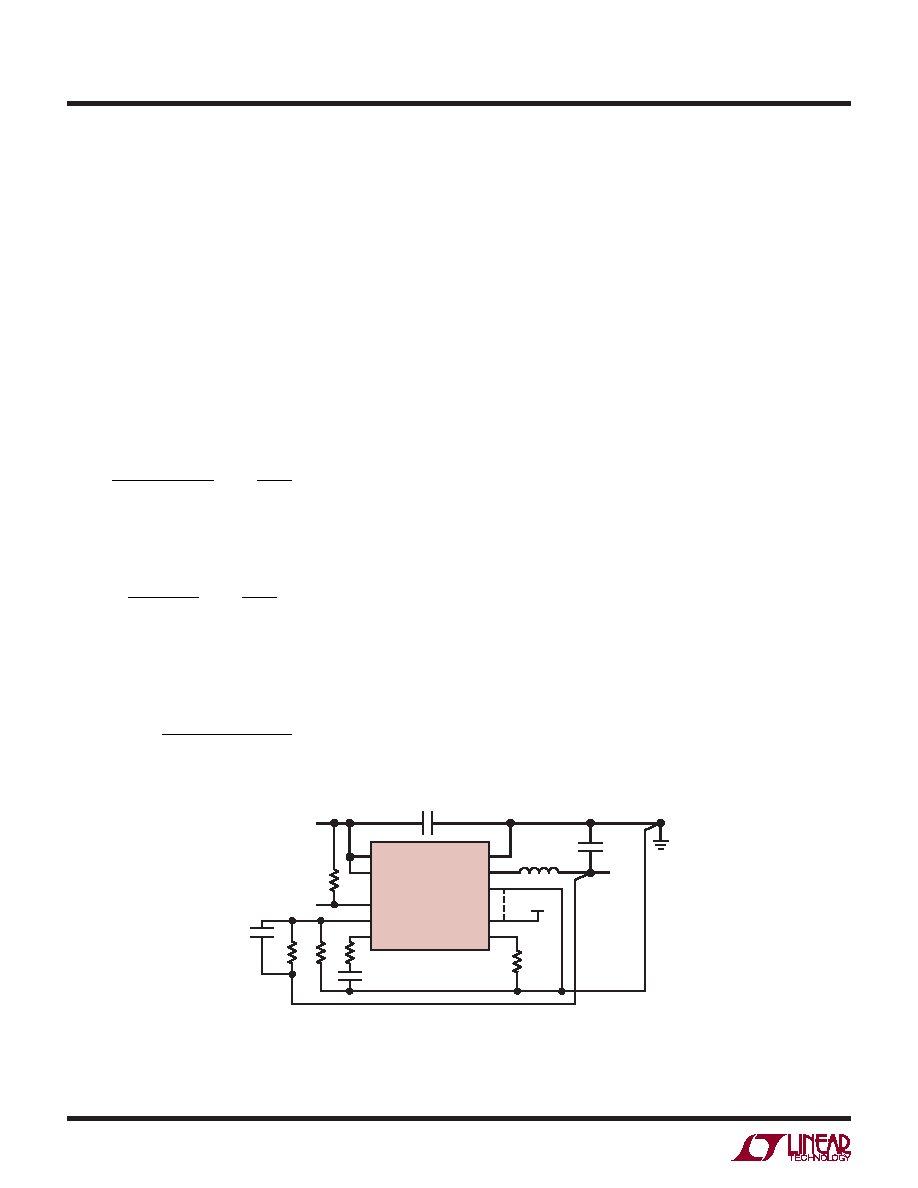
BoardLayoutConsiderations
When laying out the printed circuit board, the following
checklist should be used to ensure proper operation of
the LTC3568. These items are also illustrated graphically
in the layout diagram of Figure 6. Check the following in
your layout:
Figure6.LTC3568LayoutDiagram(SeeBoardLayoutChecklist)
PVIN
LTC3568
PGND
SW
SVIN
SGND
PGOOD
VFB
SYNC/MODE
ITH
SHDN/RT
L1
VIN
BM
PS
VIN
VOUT
R5
RT
R3
R1
R2
3568 F06
C3
BOLD LINES INDICATE HIGH CURRENT PATHS
CIN
COUT
C4
相关PDF资料 |
PDF描述 |
|---|---|
| LES015YH21N | 1-OUTPUT 15 W DC-DC REG PWR SUPPLY MODULE |
| LES015YJ18N | 1-OUTPUT 15 W DC-DC REG PWR SUPPLY MODULE |
| LES015YJ4N | 1-OUTPUT 15 W DC-DC REG PWR SUPPLY MODULE |
| LES015ZG38N | 1-OUTPUT 15 W DC-DC REG PWR SUPPLY MODULE |
| LM2320-7ERD2HF | 2-OUTPUT 50 W AC-DC REG PWR SUPPLY MODULE |
相关代理商/技术参数 |
参数描述 |
|---|---|
| LTC3569 | 制造商:LINER 制造商全称:Linear Technology 功能描述:7-Channel Confi gurable High Power PMIC |
| LTC3569EFE | 制造商:Linear Technology 功能描述:DC/DC Converter Chip |
| LTC3569EFE#PBF | 功能描述:IC REG BUCK SYNC ADJ 16TSSOP RoHS:是 类别:集成电路 (IC) >> PMIC - 稳压器 - DC DC 开关稳压器 系列:- 标准包装:250 系列:- 类型:降压(降压) 输出类型:固定 输出数:1 输出电压:1.2V 输入电压:2.05 V ~ 6 V PWM 型:电压模式 频率 - 开关:2MHz 电流 - 输出:500mA 同步整流器:是 工作温度:-40°C ~ 85°C 安装类型:表面贴装 封装/外壳:6-UFDFN 包装:带卷 (TR) 供应商设备封装:6-SON(1.45x1) 产品目录页面:1032 (CN2011-ZH PDF) 其它名称:296-25628-2 |
| LTC3569EFE#TRPBF | 功能描述:IC REG BUCK SYNC ADJ 16TSSOP RoHS:是 类别:集成电路 (IC) >> PMIC - 稳压器 - DC DC 开关稳压器 系列:- 标准包装:2,500 系列:- 类型:降压(降压) 输出类型:固定 输出数:1 输出电压:1.2V,1.5V,1.8V,2.5V 输入电压:2.7 V ~ 20 V PWM 型:- 频率 - 开关:- 电流 - 输出:50mA 同步整流器:是 工作温度:-40°C ~ 125°C 安装类型:表面贴装 封装/外壳:10-TFSOP,10-MSOP(0.118",3.00mm 宽)裸露焊盘 包装:带卷 (TR) 供应商设备封装:10-MSOP 裸露焊盘 |
| LTC3569EFE-PBF | 制造商:LINER 制造商全称:Linear Technology 功能描述:Triple Buck Regulator With 1.2A and Two 600mA Outputs and Individual Programmable References |
发布紧急采购,3分钟左右您将得到回复。