- 您现在的位置:买卖IC网 > PDF目录80024 > LTC3569EFE#PBF (LINEAR TECHNOLOGY CORP) 2.5 A SWITCHING REGULATOR, 3000 kHz SWITCHING FREQ-MAX, PDSO16 PDF资料下载
参数资料
| 型号: | LTC3569EFE#PBF |
| 厂商: | LINEAR TECHNOLOGY CORP |
| 元件分类: | 稳压器 |
| 英文描述: | 2.5 A SWITCHING REGULATOR, 3000 kHz SWITCHING FREQ-MAX, PDSO16 |
| 封装: | 4.40 MM, LEAD FREE, PLASTIC, TSSOP-16 |
| 文件页数: | 6/26页 |
| 文件大小: | 468K |
| 代理商: | LTC3569EFE#PBF |
LTC3569
14
3569fd
APPLICATIONS INFORMATION
Operating Frequency
Selection of the operating frequency is a trade-off between
efficiency and component size. High frequency operation
allowsforsmallerinductorandcapacitorvalues.Operation
at lower frequencies improves the efficiency by reducing
internal gate charge losses but requires larger inductance
values and/or capacitance to maintain low output ripple
voltage.
Theoperatingfrequency,fCLK,oftheLTC3569isdetermined
by an external resistor that is connected between the RT
pin and ground. The value of the resistor sets the ramp
current that charges and discharges an internal timing
capacitor within the oscillator. The relationship between
oscillator frequency and RT is calculated by the following
equation:
RT = (5.1855 1011) (fCLK)–1.027
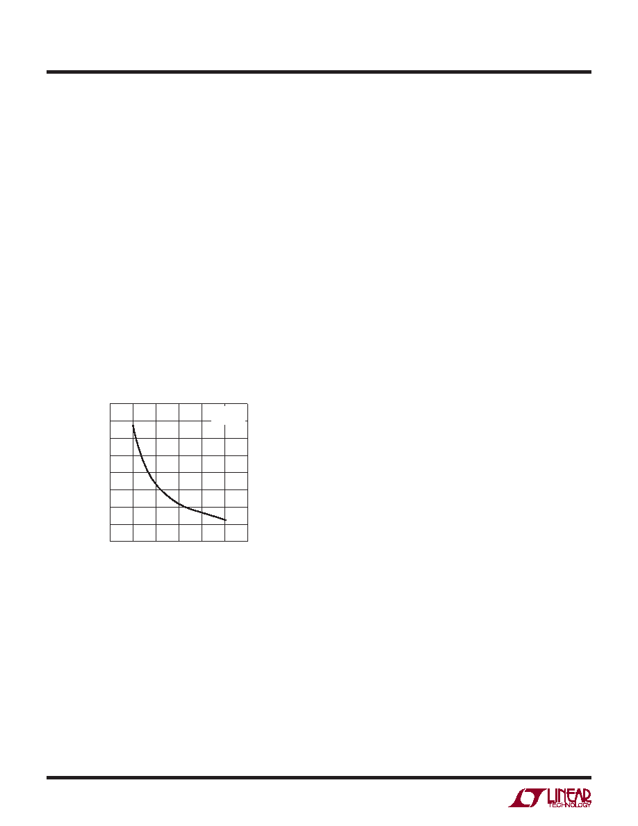
Or may be selected following the graph in Figure 4.
Minimum On-Time And Duty-Cycle
The maximum usable operating frequency is limited by
the minimum on-time and the required duty cycle. In buck
regulators, the duty cycle (DC) is the ratio of output to
input voltage: DC = VOUT/VIN = tON/(tOFF + tON). At low duty
cycles, the SW node is high for a small fraction of the total
clock period. As this time period approaches the speed
of the gate drive circuits and the comparators internal to
the LTC3569, the dynamic loop response suffers. To avoid
minimum on-time issues it is recommended to adjust the
operating frequency down so as to keep the minimum
duty cycle pulse width above 80ns. Thus, the maximum
operating frequency should be selected such that the duty
cycle does not demand SW pulse widths below the mini-
mum on-time. The maximum clock frequency, fCLKMAX,
is selected from either the internal fixed frequency clock,
or a timing resistor at the RT pin, or synchronizing clock
applied to the MODE pin. The minimum on-time require-
ment is met by adhering to the following formula:
fCLKMAX = (VOUT/VIN(MAX))/tMIN-ON
For example, if VOUT is 0.8V and VIN ranges up to 5.5V,
the maximum clock frequency is limited to no more than
1.8MHz.
Mode Selection And Frequency Synchronization
The MODE pin is a multi-purpose pin which provides
mode selection and frequency synchronization. Connect-
ing this pin to SVIN enables Burst Mode operation, which
provides the best low current efficiency at the cost of a
higher output voltage ripple. When this pin is connected
to ground, pulse-skipping operation is selected which
provides the lowest output voltage and current ripple at
the cost of low current efficiency.
Synchronize the LTC3569 to an external clock signal by
tying a clock source to the MODE pin. Select the RT pin
resistance so that the internal oscillator frequency is set
to 20% lower than the applied external clock frequency to
ensure adequate slope compensation, since slope com-
pensation is derived from the internal oscillator. During
synchronization, the mode is set to pulse skipping.
TheexternalclocksourceappliedtotheMODEpinrequires
minimum low and high pulse widths of about 100ns.
Figure 4. fCLK vs RT
The minimum frequency is limited by leakage and noise
coupling due to the large resistance of RT.
If the RT pin is tied to SVIN the oscillation frequency is
fixed at 2.25MHz.
Keep excess capacitance and noise (e.g., from the SW
pins) away from the RT pin. It is recommended to remove
the GND plane beneath the RT pin trace, and to route the
RT pin PCB trace away from the SW pins.
RT (M)
0
f CLK
(MHz)
4.1
3.6
2.6
1.1
1.6
3.1
2.1
0.6
0.1
0.4
0.2
3569 F04
0.6
0.3
0.1
0.5
VIN = 3.6V
TA = 25°C
相关PDF资料 |
PDF描述 |
|---|---|
| LTC4224CMS-2#TRMPBF | 2-CHANNEL POWER SUPPLY SUPPORT CKT, PDSO10 |
| LM4041CIM-1.2Y | 1-OUTPUT TWO TERM VOLTAGE REFERENCE, 1.225 V, PDSO8 |
| LT3653IDCB#PBF | 1.2 A BATTERY CHARGE CONTROLLER, 1650 kHz SWITCHING FREQ-MAX, PDSO8 |
| LTC3388IDD-3#PBF | 0.21 A SWITCHING REGULATOR, PDSO10 |
| LM329CH#TRPBF | 1-OUTPUT TWO TERM VOLTAGE REFERENCE, 6.9 V, MBCY2 |
相关代理商/技术参数 |
参数描述 |
|---|---|
| LTC3569EFE-TRPBF | 制造商:LINER 制造商全称:Linear Technology 功能描述:Triple Buck Regulator With 1.2A and Two 600mA Outputs and Individual Programmable References |
| LTC3569EUD#PBF | 功能描述:IC REG BUCK SYNC ADJ TRPL 20QFN RoHS:是 类别:集成电路 (IC) >> PMIC - 稳压器 - DC DC 开关稳压器 系列:- 标准包装:250 系列:- 类型:降压(降压) 输出类型:固定 输出数:1 输出电压:1.2V 输入电压:2.05 V ~ 6 V PWM 型:电压模式 频率 - 开关:2MHz 电流 - 输出:500mA 同步整流器:是 工作温度:-40°C ~ 85°C 安装类型:表面贴装 封装/外壳:6-UFDFN 包装:带卷 (TR) 供应商设备封装:6-SON(1.45x1) 产品目录页面:1032 (CN2011-ZH PDF) 其它名称:296-25628-2 |
| LTC3569EUD#TRPBF | 功能描述:IC REG BUCK SYNC ADJ TRPL 20QFN RoHS:是 类别:集成电路 (IC) >> PMIC - 稳压器 - DC DC 开关稳压器 系列:- 标准包装:2,500 系列:- 类型:降压(降压) 输出类型:固定 输出数:1 输出电压:1.2V,1.5V,1.8V,2.5V 输入电压:2.7 V ~ 20 V PWM 型:- 频率 - 开关:- 电流 - 输出:50mA 同步整流器:是 工作温度:-40°C ~ 125°C 安装类型:表面贴装 封装/外壳:10-TFSOP,10-MSOP(0.118",3.00mm 宽)裸露焊盘 包装:带卷 (TR) 供应商设备封装:10-MSOP 裸露焊盘 |
| LTC3569EUDC#PBF | 功能描述:IC REG BUCK SYNC ADJ TRPL 20QFN RoHS:是 类别:集成电路 (IC) >> PMIC - 稳压器 - DC DC 开关稳压器 系列:- 标准包装:2,500 系列:- 类型:降压(降压) 输出类型:固定 输出数:1 输出电压:1.2V,1.5V,1.8V,2.5V 输入电压:2.7 V ~ 20 V PWM 型:- 频率 - 开关:- 电流 - 输出:50mA 同步整流器:是 工作温度:-40°C ~ 125°C 安装类型:表面贴装 封装/外壳:10-TFSOP,10-MSOP(0.118",3.00mm 宽)裸露焊盘 包装:带卷 (TR) 供应商设备封装:10-MSOP 裸露焊盘 |
| LTC3569EUDC#TRPBF | 功能描述:IC REG BUCK SYNC ADJ TRPL 20QFN RoHS:是 类别:集成电路 (IC) >> PMIC - 稳压器 - DC DC 开关稳压器 系列:- 标准包装:2,500 系列:- 类型:降压(降压) 输出类型:固定 输出数:1 输出电压:1.2V,1.5V,1.8V,2.5V 输入电压:2.7 V ~ 20 V PWM 型:- 频率 - 开关:- 电流 - 输出:50mA 同步整流器:是 工作温度:-40°C ~ 125°C 安装类型:表面贴装 封装/外壳:10-TFSOP,10-MSOP(0.118",3.00mm 宽)裸露焊盘 包装:带卷 (TR) 供应商设备封装:10-MSOP 裸露焊盘 |
发布紧急采购,3分钟左右您将得到回复。