- 您现在的位置:买卖IC网 > PDF目录80024 > LTC3569EFE#PBF (LINEAR TECHNOLOGY CORP) 2.5 A SWITCHING REGULATOR, 3000 kHz SWITCHING FREQ-MAX, PDSO16 PDF资料下载
参数资料
| 型号: | LTC3569EFE#PBF |
| 厂商: | LINEAR TECHNOLOGY CORP |
| 元件分类: | 稳压器 |
| 英文描述: | 2.5 A SWITCHING REGULATOR, 3000 kHz SWITCHING FREQ-MAX, PDSO16 |
| 封装: | 4.40 MM, LEAD FREE, PLASTIC, TSSOP-16 |
| 文件页数: | 8/26页 |
| 文件大小: | 468K |
| 代理商: | LTC3569EFE#PBF |
LTC3569
16
3569fd
APPLICATIONS INFORMATION
Input/Output Capacitor Selection
Use low equivalent series resistance (ESR) ceramic
capacitors at the switching regulator outputs as well as
at the input supply pins. It is recommended to use only
X5R or X7R ceramic capacitors because they retain their
capacitance over wider voltage and temperature ranges
than other ceramic types.
For good transient response and stability the input and
output capacitors should retain at least 50% of rated ca-
pacitance value over temperature and bias voltage. Check
with capacitor data sheets to ensure that bias voltage and
temperature derating is taken into account when selecting
capacitors.
In continuous mode, the input supply current is a square
waveofdutycycleVOUT/VIN.Themaximuminputcapacitor
ripple current is approximated by:
CIN required IRMS ≈ IOUT(MAX)(VOUT(VIN–VOUT))1/2/VIN
This formula’s maximum is approximately IRMS =
IOUT(MAX)/2.
In an output short-circuit situation, the input capacitor
ripple current is approximately:
CIN required IRMS ≈ IPK /√3
Thus, the ripple current in an output short-circuit is about
2.5 times larger than for nominal operation. Take care
in selecting the input capacitor so as not to exceed the
capacitor manufacturer’s specification for self heating due
to the ripple current.
Two factors influence the selection of the output capacitor.
The first is load voltage droop, VDROOP, the second is the
output capacitor ESR effect on ripple voltage.
Load voltage droops on a load current step,
IOUT, where
the output capacitor supports the output voltage for typi-
cally 2 to 3 clock cycles until the inductor current charges
up to the load step current level. A good estimate of output
capacitor value required to maintain a droop of less than
VDROOP is given by:
COUT ≈ 2.5IOUT/(fCLKVDROOP)
Thesecondfactorthatinfluencestheselectionoftheoutput
capacitoristheeffectofoutputcapacitorESRontheoutput
voltage ripple as a result of the inductor ripple current.
The amplitude of voltage ripple,
VOUT, is determined by:
VOUT ≈ IL(ESR + 1/(8fCLKCOUT))
Where
IL is the ripple current in the inductor, and ESR
is the equivalent series resistance of the output capacitor.
Using ceramic capacitors, this voltage ripple is usually
negligible.
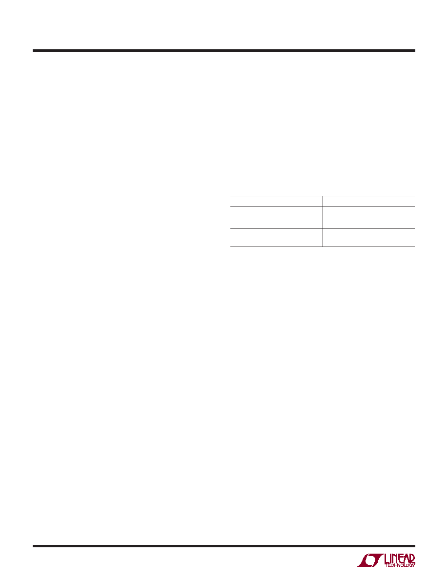
Table 2. Capacitors
VENDOR/PART NUMBER
VALUE (F)
Murata: GRM21BR71A106KE51
10
Murata: 06036D475KAT
4.7
TDK: C1608X5R0J106M
C1608X7R1C105K
10
1
Printed Circuit Board Layout Considerations
There are three main considerations to take into account
while designing a PCB layout for the LTC3569. The first
consideration is regarding switching noise coupling onto
the FB pin traces and the RT pin trace, or causing radiated
electromagnetic induction (EMI). The noise is mitigated
by placing the inductors and input decoupling capacitors
as close as possible to the LTC3569. Furthermore, careful
placement of a contiguous ground plane directly under
the high frequency switching node traces of the LTC3569
mitigates EMI; since high frequency eddy currents follow
the ground plane in loops. The larger the area of the cur-
rent return loops the larger EMI that is radiated. Placing
input decoupling capacitors close to the corresponding
PVIN/PGND pins directly reduces the area (and therefore
the inductance) of ground returns. Also, place a group of
vias directly under the grounded backside of the package
leading to an internal ground plane. Place the ground
plane on the second layer of the PCB to minimize parasitic
inductance.
相关PDF资料 |
PDF描述 |
|---|---|
| LTC4224CMS-2#TRMPBF | 2-CHANNEL POWER SUPPLY SUPPORT CKT, PDSO10 |
| LM4041CIM-1.2Y | 1-OUTPUT TWO TERM VOLTAGE REFERENCE, 1.225 V, PDSO8 |
| LT3653IDCB#PBF | 1.2 A BATTERY CHARGE CONTROLLER, 1650 kHz SWITCHING FREQ-MAX, PDSO8 |
| LTC3388IDD-3#PBF | 0.21 A SWITCHING REGULATOR, PDSO10 |
| LM329CH#TRPBF | 1-OUTPUT TWO TERM VOLTAGE REFERENCE, 6.9 V, MBCY2 |
相关代理商/技术参数 |
参数描述 |
|---|---|
| LTC3569EFE-TRPBF | 制造商:LINER 制造商全称:Linear Technology 功能描述:Triple Buck Regulator With 1.2A and Two 600mA Outputs and Individual Programmable References |
| LTC3569EUD#PBF | 功能描述:IC REG BUCK SYNC ADJ TRPL 20QFN RoHS:是 类别:集成电路 (IC) >> PMIC - 稳压器 - DC DC 开关稳压器 系列:- 标准包装:250 系列:- 类型:降压(降压) 输出类型:固定 输出数:1 输出电压:1.2V 输入电压:2.05 V ~ 6 V PWM 型:电压模式 频率 - 开关:2MHz 电流 - 输出:500mA 同步整流器:是 工作温度:-40°C ~ 85°C 安装类型:表面贴装 封装/外壳:6-UFDFN 包装:带卷 (TR) 供应商设备封装:6-SON(1.45x1) 产品目录页面:1032 (CN2011-ZH PDF) 其它名称:296-25628-2 |
| LTC3569EUD#TRPBF | 功能描述:IC REG BUCK SYNC ADJ TRPL 20QFN RoHS:是 类别:集成电路 (IC) >> PMIC - 稳压器 - DC DC 开关稳压器 系列:- 标准包装:2,500 系列:- 类型:降压(降压) 输出类型:固定 输出数:1 输出电压:1.2V,1.5V,1.8V,2.5V 输入电压:2.7 V ~ 20 V PWM 型:- 频率 - 开关:- 电流 - 输出:50mA 同步整流器:是 工作温度:-40°C ~ 125°C 安装类型:表面贴装 封装/外壳:10-TFSOP,10-MSOP(0.118",3.00mm 宽)裸露焊盘 包装:带卷 (TR) 供应商设备封装:10-MSOP 裸露焊盘 |
| LTC3569EUDC#PBF | 功能描述:IC REG BUCK SYNC ADJ TRPL 20QFN RoHS:是 类别:集成电路 (IC) >> PMIC - 稳压器 - DC DC 开关稳压器 系列:- 标准包装:2,500 系列:- 类型:降压(降压) 输出类型:固定 输出数:1 输出电压:1.2V,1.5V,1.8V,2.5V 输入电压:2.7 V ~ 20 V PWM 型:- 频率 - 开关:- 电流 - 输出:50mA 同步整流器:是 工作温度:-40°C ~ 125°C 安装类型:表面贴装 封装/外壳:10-TFSOP,10-MSOP(0.118",3.00mm 宽)裸露焊盘 包装:带卷 (TR) 供应商设备封装:10-MSOP 裸露焊盘 |
| LTC3569EUDC#TRPBF | 功能描述:IC REG BUCK SYNC ADJ TRPL 20QFN RoHS:是 类别:集成电路 (IC) >> PMIC - 稳压器 - DC DC 开关稳压器 系列:- 标准包装:2,500 系列:- 类型:降压(降压) 输出类型:固定 输出数:1 输出电压:1.2V,1.5V,1.8V,2.5V 输入电压:2.7 V ~ 20 V PWM 型:- 频率 - 开关:- 电流 - 输出:50mA 同步整流器:是 工作温度:-40°C ~ 125°C 安装类型:表面贴装 封装/外壳:10-TFSOP,10-MSOP(0.118",3.00mm 宽)裸露焊盘 包装:带卷 (TR) 供应商设备封装:10-MSOP 裸露焊盘 |
发布紧急采购,3分钟左右您将得到回复。