- 您现在的位置:买卖IC网 > PDF目录14798 > LTC3605EUF#PBF (Linear Technology)IC REG BUCK SYNC ADJ 5A 24QFN PDF资料下载
参数资料
| 型号: | LTC3605EUF#PBF |
| 厂商: | Linear Technology |
| 文件页数: | 9/22页 |
| 文件大小: | 0K |
| 描述: | IC REG BUCK SYNC ADJ 5A 24QFN |
| 标准包装: | 91 |
| 类型: | 降压(降压) |
| 输出类型: | 可调式 |
| 输出数: | 1 |
| 输出电压: | 0.6 V ~ 14.9 V |
| 输入电压: | 4 V ~ 15 V |
| PWM 型: | 电流模式 |
| 频率 - 开关: | 1MHz |
| 电流 - 输出: | 5A |
| 同步整流器: | 是 |
| 工作温度: | -40°C ~ 85°C |
| 安装类型: | 表面贴装 |
| 封装/外壳: | 24-WFQFN 裸露焊盘 |
| 包装: | 管件 |
| 供应商设备封装: | 24-QFN(4x4) |
| 产品目录页面: | 1335 (CN2011-ZH PDF) |
�� �
�
�LTC3605�
�OPERATION�
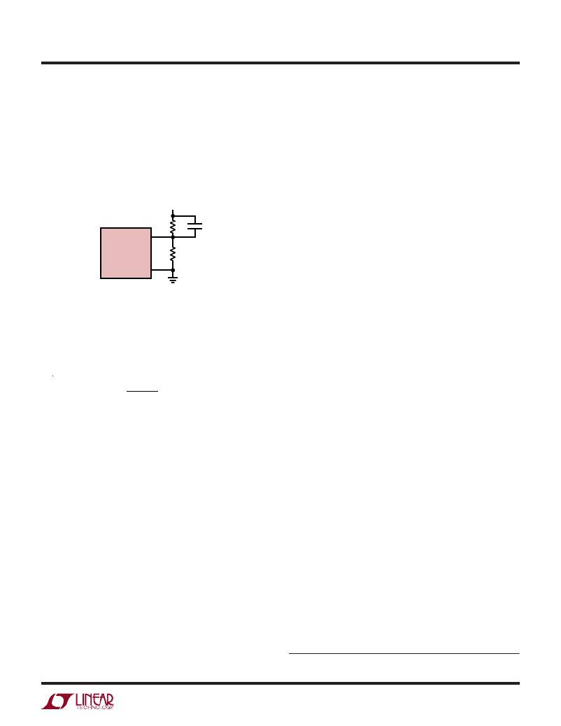
�Output� Voltage� Programming�
�The� output� voltage� is� set� by� an� external� resistive� divider�
�according� to� the� following� equation:�
�V� OUT� =� 0.6V� ?� (1� +� R2/R1)�
�The� resistive� divider� allows� the� V� FB� pin� to� sense� a� fraction�
�of� the� output� voltage� as� shown� in� Figure� 1.�
�V� OUT�
�R2� C� FF�
�FB�
�Output� Power� Good�
�When� the� LTC3605’s� output� voltage� is� within� the� ±10%�
�window� of� the� regulation� point,� which� is� reflected� back� as�
�a� V� FB� voltage� in� the� range� of� 0.54V� to� 0.66V,� the� output�
�voltage� is� good� and� the� PGOOD� pin� is� pulled� high� with� an�
�external� resistor.� Otherwise,� an� internal� open-drain� pull-�
�down� device� (12Ω)� will� pull� the� PGOOD� pin� low.� To� prevent�
�unwanted� PGOOD� glitches� during� transients� or� dynamic�
�V� OUT� changes,� the� LTC3605’s� PGOOD� falling� edge� includes�
�a� blanking� delay� of� approximately� 52� switching� cycles.�
�LTC3605�
�R1�
�Multiphase� Operation�
�Frequency� (Hz)� =�
�SGND�
�3605� F01�
�Figure� 1.� Setting� the� Output� Voltage�
�Programming� Switching� Frequency�
�Connecting� a� resistor� from� the� RT� pin� to� SGND� programs�
�the� switching� frequency� from� 800kHz� to� 4MHz� according�
�to� the� following� formula:�
�1.6e11�
�R� T� (� W� )�
�The� internal� PLL� has� a� synchronization� range� of� ±30%�
�around� its� programmed� frequency.� Therefore,� during�
�external� clock� synchronization� be� sure� that� the� external�
�clock� frequency� is� within� this� ±30%� range� of� the� RT� pro-�
�grammed� frequency.�
�Output� Voltage� Tracking� and� Soft-Start�
�The� LTC3605� allows� the� user� to� program� its� output� voltage�
�ramp� rate� by� means� of� the� TRACK/SS� pin.� An� internal� 2μA�
�pulls� up� the� TRACK/SS� pin� to� INTV� CC� .� Putting� an� external�
�capacitor� on� TRACK/SS� enables� soft� starting� the� output�
�to� prevent� current� surge� on� the� input� supply.� For� output�
�tracking� applications,� TRACK/SS� can� be� externally� driven�
�by� another� voltage� source.� From� 0V� to� 0.6V,� the� TRACK/SS�
�voltage� will� override� the� internal� 0.6V� reference� input� to� the�
�error� amplifier,� thus� regulating� the� feedback� voltage� to� that�
�of� TRACK/SS� pins.� During� this� start-up� time,� the� LTC3605�
�will� operate� in� discontinuous� mode.� When� TRACK/SS� is�
�above� 0.6V,� tracking� is� disabled� and� the� feedback� voltage�
�will� regulate� to� the� internal� reference� voltage.�
�For� output� loads� that� demand� more� than� 5A� of� current,�
�multiple� LTC3605s� can� be� cascaded� to� run� out� of� phase�
�to� provide� more� output� current.� The� CLKIN� pin� allows�
�the� LTC3605� to� synchronize� to� an� external� clock� (±50%�
�of� frequency� programmed� by� RT)� and� the� internal� phase-�
�locked-loop� allows� the� LTC3605� to� lock� onto� CLKIN’s�
�phase� as� well.� The� CLKOUT� signal� can� be� connected� to� the�
�CLKIN� pin� of� the� following� LTC3605� stage� to� line� up� both�
�the� frequency� and� the� phase� of� the� entire� system.� Tying�
�the� PHMODE� pin� to� INTV� CC� ,� SGND� or� INTV� CC� /2� generates�
�a� phase� difference� (between� CLKIN� and� CLKOUT)� of� 180�
�degrees,� 120� degrees,� or� 90� degrees� respectively,� which�
�corresponds� to� 2-phase,� 3-phase� or� 4-phase� operation.� A�
�total� of� 12� phases� can� be� cascaded� to� run� simultaneously�
�out� of� phase� with� respect� to� each� other� by� programming�
�the� PHMODE� pin� of� each� LTC3605� to� different� levels.�
�Internal/External� ITH� Compensation�
�During� single� phase� operation,� the� user� can� simplify�
�the� loop� compensation� by� tying� the� I� TH� pin� to� INTV� CC� to�
�enable� internal� compensation.� This� connects� an� internal�
�30k� resistor� in� series� with� a� 40pF� capacitor� to� the� output�
�of� the� error� amplifier� (internal� ITH� compensation� point)�
�while� also� activating� output� voltage� positioning� such�
�that� the� output� voltage� will� be� 1.5%� above� regulation� at�
�no� load� and� 1.5%� below� regulation� at� full� load.� This� is� a�
�trade-off� for� simplicity� instead� of� OPTI-LOOP� ?� optimiza-�
�tion,� where� ITH� components� are� external� and� are� selected�
�to� optimize� the� loop� transient� response� with� minimum�
�output� capacitance.�
�OPTI-LOOP� is� a� registered� trademark� of� Linear� Technology� Corporation.�
�3605fc�
�9�
�相关PDF资料 |
PDF描述 |
|---|---|
| LT3972EDD#PBF | IC REG BUCK ADJ 3.5A 10DFN |
| LT1956IGN#PBF | IC REG BUCK ADJ 1.5A 16SSOP |
| LTC3414EFE#PBF | IC REG BUCK SYNC ADJ 4A 20TSSOP |
| EBC40DRTI-S13 | CONN EDGECARD 80POS .100 EXTEND |
| LT1054IS8#PBF | IC REG SWITCHD CAP DBL INV 8SOIC |
相关代理商/技术参数 |
参数描述 |
|---|---|
| LTC3605IUF#PBF | 功能描述:IC REG BUCK SYNC ADJ 5A 24QFN RoHS:是 类别:集成电路 (IC) >> PMIC - 稳压器 - DC DC 开关稳压器 系列:- 设计资源:Design Support Tool 标准包装:1 系列:- 类型:升压(升压) 输出类型:固定 输出数:1 输出电压:3V 输入电压:0.75 V ~ 2 V PWM 型:- 频率 - 开关:- 电流 - 输出:100mA 同步整流器:是 工作温度:-40°C ~ 85°C 安装类型:表面贴装 封装/外壳:SOT-23-5 细型,TSOT-23-5 包装:剪切带 (CT) 供应商设备封装:TSOT-23-5 其它名称:AS1323-BTTT-30CT |
| LTC3605IUF#TRPBF | 功能描述:IC REG BUCK SYNC ADJ 5A 24QFN RoHS:是 类别:集成电路 (IC) >> PMIC - 稳压器 - DC DC 开关稳压器 系列:- 设计资源:Design Support Tool 标准包装:1 系列:- 类型:升压(升压) 输出类型:固定 输出数:1 输出电压:3V 输入电压:0.75 V ~ 2 V PWM 型:- 频率 - 开关:- 电流 - 输出:100mA 同步整流器:是 工作温度:-40°C ~ 85°C 安装类型:表面贴装 封装/外壳:SOT-23-5 细型,TSOT-23-5 包装:剪切带 (CT) 供应商设备封装:TSOT-23-5 其它名称:AS1323-BTTT-30CT |
| LTC3606BEDD#PBF | 功能描述:IC REG BUCK SYNC ADJ 0.8A 8DFN RoHS:是 类别:集成电路 (IC) >> PMIC - 稳压器 - DC DC 开关稳压器 系列:- 标准包装:250 系列:- 类型:降压(降压) 输出类型:固定 输出数:1 输出电压:1.2V 输入电压:2.05 V ~ 6 V PWM 型:电压模式 频率 - 开关:2MHz 电流 - 输出:500mA 同步整流器:是 工作温度:-40°C ~ 85°C 安装类型:表面贴装 封装/外壳:6-UFDFN 包装:带卷 (TR) 供应商设备封装:6-SON(1.45x1) 产品目录页面:1032 (CN2011-ZH PDF) 其它名称:296-25628-2 |
| LTC3606BEDD#PBF | 制造商:Linear Technology 功能描述:IC SYNC STEP-DOWN DC/DC CONVERTER DFN8 |
| LTC3606BEDD#TRPBF | 功能描述:IC REG BUCK SYNC ADJ 0.8A 8DFN RoHS:是 类别:集成电路 (IC) >> PMIC - 稳压器 - DC DC 开关稳压器 系列:- 标准包装:2,500 系列:- 类型:升压(升压) 输出类型:可调式 输出数:1 输出电压:1.24 V ~ 30 V 输入电压:1.5 V ~ 12 V PWM 型:电流模式,混合 频率 - 开关:600kHz 电流 - 输出:500mA 同步整流器:无 工作温度:-40°C ~ 85°C 安装类型:表面贴装 封装/外壳:8-SOIC(0.154",3.90mm 宽) 包装:带卷 (TR) 供应商设备封装:8-SOIC |
发布紧急采购,3分钟左右您将得到回复。