- 您现在的位置:买卖IC网 > PDF目录30770 > LTC3615EFE-1#TRPBF (LINEAR TECHNOLOGY CORP) SWITCHING REGULATOR, PDSO24 PDF资料下载
参数资料
| 型号: | LTC3615EFE-1#TRPBF |
| 厂商: | LINEAR TECHNOLOGY CORP |
| 元件分类: | 稳压器 |
| 英文描述: | SWITCHING REGULATOR, PDSO24 |
| 封装: | 4.40 MM, LEAD FREE, PLASTIC, TSSOP-24 |
| 文件页数: | 27/32页 |
| 文件大小: | 585K |
| 代理商: | LTC3615EFE-1#TRPBF |
第1页第2页第3页第4页第5页第6页第7页第8页第9页第10页第11页第12页第13页第14页第15页第16页第17页第18页第19页第20页第21页第22页第23页第24页第25页第26页当前第27页第28页第29页第30页第31页第32页
LTC3615/LTC3615-1
4
3615fa
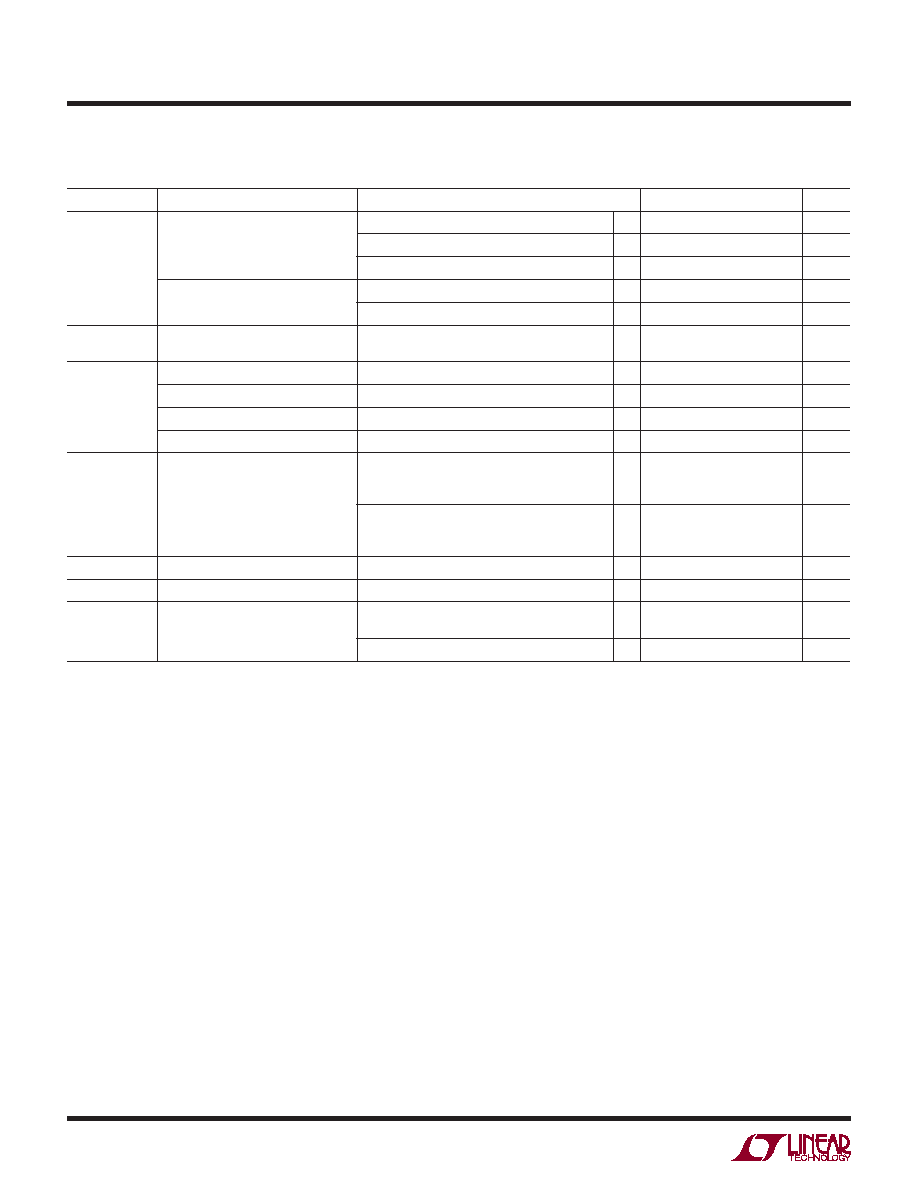
SYMBOL
PARAMETER
CONDITIONS
MIN
TYP
MAX
UNITS
SW1–SW2
Output Phase Shift Between SW1
and SW2 (LTC3615)
VPHASE < 0.15 SVIN
0Deg
0.35 SVIN < VPHASE < 0.65 SVIN
90
Deg
VPHASE > 0.85 SVIN
180
Deg
Output Phase Shift Between SW1
and SW2 (LTC3615-1)
VPHASE < 0.65 SVIN
140
Deg
VPHASE > 0.85 SVIN
180
Deg
VSRLIM
Voltage at SRLIM to Enable DDR
Mode
(Note 9)
SVIN – 0.3
V
VMODE
(Note 9)
Internal Burst Mode Operation
0.3
V
Pulse-Skipping Mode
SVIN – 0.3
V
Forced Continuous Mode
1.1
SVIN 0.58
V
External Burst Mode Operation
0.5
0.85
V
PGOOD
Power Good Voltage Windows
TRACK/SSx = SVIN, Entering Window
VFBx Ramping Up
VFBx Ramping Down
–3.5
3.5
–6
6
%
TRACK/SSx = SVIN, Leaving Window
VFBx Ramping Up
VFBx Ramping Down
9
–9
11
–11
%
tPGOOD
Power Good Blanking Time
Entering/Leaving Window
70
105
140
μs
RPGOOD
Power Good Pull-Down On-Resistance I = 10mA
8
12
30
Ω
VRUN
Enable Pin
Input High
Input Low
l
1
0.4
V
Pull-Down Resistance
4
MΩ
ELECTRICAL CHARACTERISTICS
Note 1: Stresses beyond those listed under Absolute Maximum Ratings
may cause permanent damage to the device. Exposure to any Absolute
Maximum Rating condition for extended periods may affect device
reliability and lifetime.
Note 2: The LTC3615/LTC3615-1 are tested under pulsed load conditions
such that TJ ≈ TA. The LTC3615E/LTC3615E-1 are guaranteed to meet
performance specications over the 0°C to 85°C operating junction
temperature range. Specications over the –40°C to 125°C operating
junction temperature range are assured by design, characterization and
correlation with statistical process controls. The LTC3615I/LTC3615I-1 are
guaranteed to meet specications over the full –40°C to 125°C operating
junction temperature range. Note that the maximum ambient temperature
is determined by specic operating conditions in conjunction with board
layout, the rated package thermal resistance and other environmental
factors. Note that the maximum ambient temperature consistent with
these specications is determined by specic operating conditions in
conjunction with board layout, the rated package thermal impedance
and other environmental factors. The junction temperature (TJ, in °C) is
calculated from the ambient temperature
(TA, in °C) and power dissipation (PD, in watts) according to the formula:
TJ = TA + (PD θJA)
where θJA (in °C/W) is the package thermal impedence.
Note 3: This parameter is tested in a feedback loop which servos VFB1,2 to
the midpoint for the error amplier (VITH1,2 = 0.75V).
Note 4: External compensation on ITH pin.
Note 5: Tying the ITH pin to SVIN enables internal compensation and AVP
mode for the selected channel.
Note 6: Dynamic supply current is higher due to the internal gate charge
being delivered at the switching frequency.
Note 7: See description of the TRACK/SS pin in the Pin Functions section.
Note 8: When sourcing current, the average output current is dened
as owing out of the SW pin. When sinking current, the average output
current is dened as owing into the SW pin. Sinking mode requires the
use of forced continuous mode.
Note 9: See description of the MODE pin in the Pin Functions section.
Note 10: Guaranteed by design and correlation to wafer level
measurements for QFN packages.
Note 11: This IC includes overtemperature protection that is intended
to protect the device during momentary overload conditions. Junction
temperature will exceed 125°C when overtemperature protection is active.
Continuous operation above the specied maximum operating junction
temperature may impair device reliability or permanently damage the
device.
The
l denotes the specications which apply over the full operating
junction temperature range, otherwise specications are at TA = 25°C (Note 2), SVIN = PVINx = 3.3V, RT = 178k, RSRLIM = 40.2k, unless
otherwise specied (Note 2).
相关PDF资料 |
PDF描述 |
|---|---|
| LTC3615IUF-1#PBF | SWITCHING REGULATOR, PQCC24 |
| LTC3615EUF#PBF | SWITCHING REGULATOR, PQCC24 |
| LTC3615EFE#PBF | SWITCHING REGULATOR, PDSO24 |
| LTC3615IFE-1#PBF | SWITCHING REGULATOR, PDSO24 |
| LTC3615EUF#TRPBF | SWITCHING REGULATOR, PQCC24 |
相关代理商/技术参数 |
参数描述 |
|---|---|
| LTC3615EUF#PBF | 功能描述:IC REG BUCK SYNC ADJ 3A DL 24QFN RoHS:是 类别:集成电路 (IC) >> PMIC - 稳压器 - DC DC 开关稳压器 系列:- 标准包装:250 系列:- 类型:降压(降压) 输出类型:固定 输出数:1 输出电压:1.2V 输入电压:2.05 V ~ 6 V PWM 型:电压模式 频率 - 开关:2MHz 电流 - 输出:500mA 同步整流器:是 工作温度:-40°C ~ 85°C 安装类型:表面贴装 封装/外壳:6-UFDFN 包装:带卷 (TR) 供应商设备封装:6-SON(1.45x1) 产品目录页面:1032 (CN2011-ZH PDF) 其它名称:296-25628-2 |
| LTC3615EUF#TRPBF | 功能描述:IC REG BUCK SYNC ADJ 3A DL 24QFN RoHS:是 类别:集成电路 (IC) >> PMIC - 稳压器 - DC DC 开关稳压器 系列:- 设计资源:Design Support Tool 标准包装:1 系列:- 类型:升压(升压) 输出类型:固定 输出数:1 输出电压:3V 输入电压:0.75 V ~ 2 V PWM 型:- 频率 - 开关:- 电流 - 输出:100mA 同步整流器:是 工作温度:-40°C ~ 85°C 安装类型:表面贴装 封装/外壳:SOT-23-5 细型,TSOT-23-5 包装:剪切带 (CT) 供应商设备封装:TSOT-23-5 其它名称:AS1323-BTTT-30CT |
| LTC3615EUF-1#PBF | 功能描述:IC REG BUCK SYNC ADJ 3A DL 24QFN RoHS:是 类别:集成电路 (IC) >> PMIC - 稳压器 - DC DC 开关稳压器 系列:- 标准包装:250 系列:- 类型:降压(降压) 输出类型:固定 输出数:1 输出电压:1.2V 输入电压:2.05 V ~ 6 V PWM 型:电压模式 频率 - 开关:2MHz 电流 - 输出:500mA 同步整流器:是 工作温度:-40°C ~ 85°C 安装类型:表面贴装 封装/外壳:6-UFDFN 包装:带卷 (TR) 供应商设备封装:6-SON(1.45x1) 产品目录页面:1032 (CN2011-ZH PDF) 其它名称:296-25628-2 |
| LTC3615EUF-1#TRPBF | 功能描述:IC REG BUCK SYNC ADJ 3A DL 24QFN RoHS:是 类别:集成电路 (IC) >> PMIC - 稳压器 - DC DC 开关稳压器 系列:- 设计资源:Design Support Tool 标准包装:1 系列:- 类型:升压(升压) 输出类型:固定 输出数:1 输出电压:3V 输入电压:0.75 V ~ 2 V PWM 型:- 频率 - 开关:- 电流 - 输出:100mA 同步整流器:是 工作温度:-40°C ~ 85°C 安装类型:表面贴装 封装/外壳:SOT-23-5 细型,TSOT-23-5 包装:剪切带 (CT) 供应商设备封装:TSOT-23-5 其它名称:AS1323-BTTT-30CT |
| LTC3615EUFPBF | 制造商:Linear Technology 功能描述:Dual 4MHz 3A Synch Step-Down DC/DC QFN24 |
发布紧急采购,3分钟左右您将得到回复。