- 您现在的位置:买卖IC网 > PDF目录15314 > LTC3703EGN#TR (Linear Technology)IC REG CTRLR BST PWM VM 16-SSOP PDF资料下载
参数资料
| 型号: | LTC3703EGN#TR |
| 厂商: | Linear Technology |
| 文件页数: | 9/34页 |
| 文件大小: | 0K |
| 描述: | IC REG CTRLR BST PWM VM 16-SSOP |
| 标准包装: | 2,500 |
| PWM 型: | 电压模式 |
| 输出数: | 1 |
| 频率 - 最大: | 330kHz |
| 占空比: | 96% |
| 电源电压: | 9.3 V ~ 15 V |
| 降压: | 是 |
| 升压: | 是 |
| 回扫: | 无 |
| 反相: | 无 |
| 倍增器: | 无 |
| 除法器: | 无 |
| Cuk: | 无 |
| 隔离: | 无 |
| 工作温度: | -40°C ~ 85°C |
| 封装/外壳: | 16-SSOP(0.154",3.90mm 宽) |
| 包装: | 带卷 (TR) |
第1页第2页第3页第4页第5页第6页第7页第8页当前第9页第10页第11页第12页第13页第14页第15页第16页第17页第18页第19页第20页第21页第22页第23页第24页第25页第26页第27页第28页第29页第30页第31页第32页第33页第34页
�� �
�
�LTC3703�
�OPERATION�
�(Refer� to� Functional� Diagram)�
�20μs/DIV�
�V� OUT� =� 12V�
�dropinthefeedbackvoltagerelativetothereference.The�
�COMP� voltage� then� rises,� increasing� the� duty� ratio� until�
�the� output� feedback� voltage� again� matches� the� reference�
�voltage.� In� normal� operation,� the� top� MOSFET� is� turned�
�on� when� the� RS� latch� is� set� by� the� on-chip� oscillator� and�
�is� turned� off� when� the� PWM� comparator� trips� and� resets�
�the� latch.� The� PWM� comparator� trips� at� the� proper� duty�
�ratio� by� comparing� the� error� amplifier� output� (after� being�
�“compensated”� by� the� line� feedforward� multiplier)� to� a�
�sawtooth� waveform� generated� by� the� oscillator.� When� the�
�top� MOSFET� is� turned� off,� the� bottom� MOSFET� is� turned�
�on� until� the� next� cycle� begins� or,� if� pulse-skip� mode� op-�
�eration� is� enabled,� until� the� inductor� current� reverses� as�
�determined� by� the� reverse� current� comparator.� MAX� and�
�MIN� comparators� ensure� that� the� output� never� exceed�
�±5%� of� nominal� value� by� monitoring� V� FB� and� forcing� the�
�output� back� into� regulation� quickly� by� either� keeping� the� top�
�MOSFET� off� or� forcing� maximum� duty� cycle.� The� operation�
�of� its� other� features—fast� transient� response,� outstanding�
�line� regulation,� strong� gate� drivers,� short-circuit� protection�
�and� shutdown/soft-start—are� described� below.�
�Fast� Transient� Response�
�The� LTC3703� uses� a� fast� 25MHz� op� amp� as� an� error� ampli-�
�fier.� This� allows� the� compensation� network� to� be� optimized�
�for� better� load� transient� response.� The� high� bandwidth� of�
�the� amplifier,� along� with� high� switching� frequencies� and�
�low� value� inductors,� allow� very� high� loop� crossover� fre-�
�quencies.� The� 800mV� internal� reference� allows� regulated�
�output� voltages� as� low� as� 800mV� without� external� level�
�shifting� amplifiers.�
�Line� Feedforward� Compensation�
�The� LTC3703� achieves� outstanding� line� transient� response�
�using� a� patented� feedforward� correction� scheme.� With�
�this� circuit� the� duty� cycle� is� adjusted� instantaneously� to�
�changes� in� input� voltage,� thereby� avoiding� unacceptable�
�overshoot� or� undershoot.� It� has� the� added� advantage� of�
�making� the� DC� loop� gain� independent� of� input� voltage.�
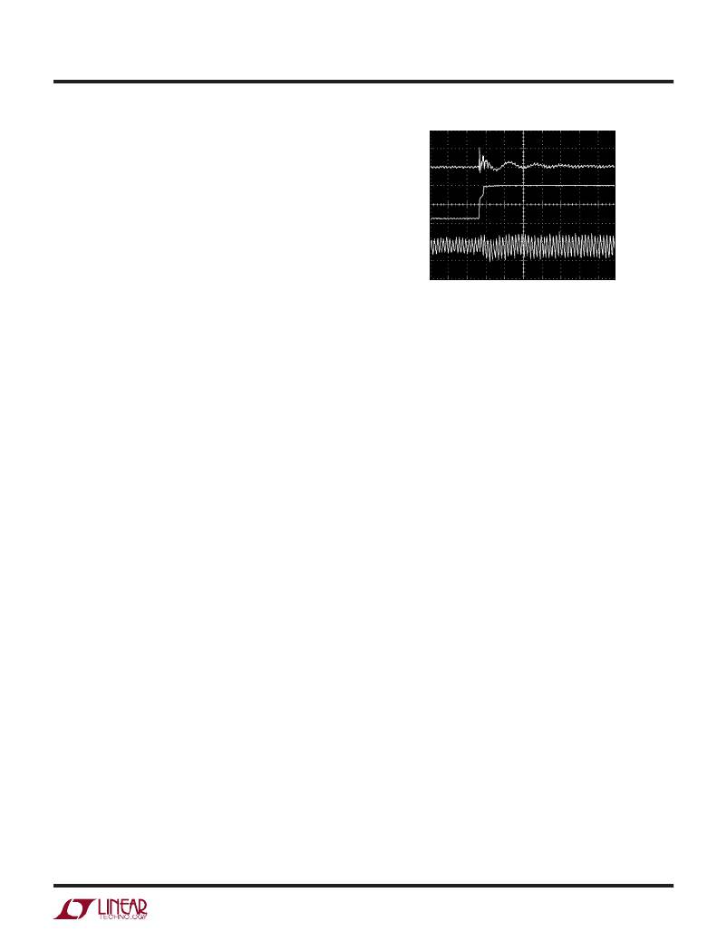
�Figure� 2� shows� how� large� transient� steps� at� the� input� have�
�little� effect� on� the� output� voltage.�
�V� OUT�
�50mV/DIV�
�V� IN�
�20V/DIV�
�I� L�
�2A/DIV�
�3703� F02�
�I� LOAD� =� 1A�
�25V� TO� 60V� V� IN� STEP�
�Figure� 2.� Line� Transient� Performance�
�Strong� Gate� Drivers�
�The� LTC3703� contains� very� low� impedance� drivers� capable�
�of� supplying� amps� of� current� to� slew� large� MOSFET� gates�
�quickly.� This� minimizes� transition� losses� and� allows� paral-�
�leling� MOSFETs� for� higher� current� applications.� A� 100V�
�floating� high� side� driver� drives� the� topside� MOSFET� and�
�a� low� side� driver� drives� the� bottom� side� MOSFET� (see�
�Figure� 3).� They� can� be� powered� from� either� a� separate�
�DC� supply� or� a� voltage� derived� from� the� input� or� output�
�voltage� (see� MOSFET� Driver� Supplies� section).� The� bottom�
�side� driver� is� supplied� directly� from� the� DRV� CC� pin.� The�
�top� MOSFET� drivers� are� biased� from� floating� bootstrap�
�capacitor,� C� B� ,� which� normally� is� recharged� during� each� off�
�cycle� through� an� external� diode� from� DRV� CC� when� the� top�
�MOSFET� turns� off.� In� pulse-skip� mode� operation,� where�
�it� is� possible� that� the� bottom� MOSFET� will� be� off� for� an�
�extended� period� of� time,� an� internal� counter� guarantees�
�that� the� bottom� MOSFET� is� turned� on� at� least� once� every�
�10� cycles� for� 10%� of� the� period� to� refresh� the� bootstrap�
�capacitor.� An� undervoltage� lockout� keeps� the� LTC3703�
�shut� down� unless� this� voltage� is� above� 8.7V.�
�The� bottom� driver� has� an� additional� feature� that� helps�
�minimize� the� possibility� of� external� MOSFET� shoot-through.�
�When� the� top� MOSFET� turns� on,� the� switch� node� dV/dt�
�pulls� up� the� bottom� MOSFET’s� internal� gate� through� the�
�Miller� capacitance,� even� when� the� bottom� driver� is� holding�
�the� gate� terminal� at� ground.� If� the� gate� is� pulled� up� high�
�enough,� shoot-through� between� the� topside� and� bottom�
�3703fc�
�9�
�相关PDF资料 |
PDF描述 |
|---|---|
| VI-220-EY-B1 | CONVERTER MOD DC/DC 5V 50W |
| CDRH4D28NP-1R8NC | INDUCTOR POWER 1.8UH 2.20A SMD |
| EEC31DRAI-S734 | CONN EDGECARD 62POS .100 R/A PCB |
| LTC1735CS-1#PBF | IC REG CTRLR BUCK PWM CM 16-SOIC |
| ESA22DRMN-S288 | CONN EDGECARD 44POS .125 EXTEND |
相关代理商/技术参数 |
参数描述 |
|---|---|
| LTC3703EGPBF | 制造商:Linear Technology 功能描述:LTC3703 100V SU/SD PS controller |
| LTC3703HGN | 制造商:Linear Technology 功能描述:DC DC Cntrlr Single-OUT Sync Step Down 9.3V to 100V Input 16-Pin SSOP N |
| LTC3703HGN#PBF | 功能描述:IC REG CTRLR BST PWM VM 16-SSOP RoHS:是 类别:集成电路 (IC) >> PMIC - 稳压器 - DC DC 切换控制器 系列:- 标准包装:2,500 系列:- PWM 型:电流模式 输出数:1 频率 - 最大:500kHz 占空比:96% 电源电压:4 V ~ 36 V 降压:无 升压:是 回扫:无 反相:无 倍增器:无 除法器:无 Cuk:无 隔离:无 工作温度:-40°C ~ 125°C 封装/外壳:24-WQFN 裸露焊盘 包装:带卷 (TR) |
| LTC3703HGN#TRPBF | 功能描述:IC REG CTRLR BST PWM VM 16-SSOP RoHS:是 类别:集成电路 (IC) >> PMIC - 稳压器 - DC DC 切换控制器 系列:- 标准包装:2,500 系列:- PWM 型:电流模式 输出数:1 频率 - 最大:500kHz 占空比:96% 电源电压:4 V ~ 36 V 降压:无 升压:是 回扫:无 反相:无 倍增器:无 除法器:无 Cuk:无 隔离:无 工作温度:-40°C ~ 125°C 封装/外壳:24-WQFN 裸露焊盘 包装:带卷 (TR) |
| LTC3703IG-5#PBF | 功能描述:IC REG CTRLR BST PWM VM 28-SSOP RoHS:是 类别:集成电路 (IC) >> PMIC - 稳压器 - DC DC 切换控制器 系列:- 标准包装:2,500 系列:- PWM 型:电流模式 输出数:1 频率 - 最大:500kHz 占空比:96% 电源电压:4 V ~ 36 V 降压:无 升压:是 回扫:无 反相:无 倍增器:无 除法器:无 Cuk:无 隔离:无 工作温度:-40°C ~ 125°C 封装/外壳:24-WQFN 裸露焊盘 包装:带卷 (TR) |
发布紧急采购,3分钟左右您将得到回复。