- 您现在的位置:买卖IC网 > PDF目录15273 > LTC3802EGN#TR (Linear Technology)IC REG CTRLR BUCK PWM VM 28-SSOP PDF资料下载
参数资料
| 型号: | LTC3802EGN#TR |
| 厂商: | Linear Technology |
| 文件页数: | 19/28页 |
| 文件大小: | 0K |
| 描述: | IC REG CTRLR BUCK PWM VM 28-SSOP |
| 标准包装: | 2,500 |
| 系列: | PolyPhase® |
| PWM 型: | 电压模式 |
| 输出数: | 2 |
| 频率 - 最大: | 850kHz |
| 占空比: | 92% |
| 电源电压: | 3 V ~ 30 V |
| 降压: | 是 |
| 升压: | 无 |
| 回扫: | 无 |
| 反相: | 无 |
| 倍增器: | 无 |
| 除法器: | 无 |
| Cuk: | 无 |
| 隔离: | 无 |
| 工作温度: | -40°C ~ 85°C |
| 封装/外壳: | 28-SSOP(0.154",3.90mm 宽) |
| 包装: | 带卷 (TR) |
第1页第2页第3页第4页第5页第6页第7页第8页第9页第10页第11页第12页第13页第14页第15页第16页第17页第18页当前第19页第20页第21页第22页第23页第24页第25页第26页第27页第28页
�� �
�
�LTC3802�
�APPLICATIO� S� I� FOR� ATIO�
�As� the� output� load� current� decreases� in� continuous� mode,�
�the� average� current� in� the� inductor� will� reach� a� point� where�
�it� drops� below� half� the� ripple� current.� At� this� point,� the�
�current� in� the� inductor� will� reverse� during� a� portion� of� the�
�switching� cycle,� or� begin� to� flow� from� the� output� back� to�
�the� input.� This� does� not� adversely� affect� regulation,� but�
�does� cause� additional� losses� as� a� portion� of� the� inductor�
�To� minimize� the� switching� loss� and� reverse� current� flow� at�
�light� loads,� the� LTC3802� switches� to� a� second� mode� of�
�operation:� Burst� Mode� operation� (Figure� 5b).� In� Burst�
�Mode� operation,� at� the� end� of� the� QB� cycle,� if� the� inductor�
�current� approaches� zero� or� goes� negative,� the� LTC3802�
�turns� off� both� drivers.� The� actual� cutoff� threshold� is�
�proportional� to� the� I� MAX� setting� and� is� equal� to:�
�current� flows� back� and� forth� through� the� resistive� power�
�switches,� giving� away� a� little� more� power� each� time� and�
�lowering� the� efficiency.� There� are� some� benefits� to� allow-�
�–�
�V� IMAX�
�100�
�–� 3� mV�
�ing� this� reverse� current� flow:� the� circuit� will� maintain�
�regulation� even� if� the� load� current� drops� to� zero� and� the�
�output� ripple� voltage� and� frequency� remain� constant� at� all�
�loads,� easing� filtering� requirements.� However,� continuous�
�mode� at� low� output� current� does� cause� losses� in� effi-�
�ciency.� A� portion� of� the� inductor� current� flows� back� and�
�forth� through� the� resistive� power� switches,� causing� I� 2� R�
�losses.� The� drivers� continue� to� switch� QT� and� QB� on� and�
�off� once� a� cycle.� Each� time� an� external� MOSFET� is� turned�
�on,� the� internal� driver� must� charge� its� gate� to� a� potential�
�above� the� MOSFET’s� source� voltage;� when� the� MOSFET� is�
�turned� off,� that� charge� is� lost� to� ground� or� SW.� At� the� high�
�switching� frequencies,� the� lost� gate� charges� can� add� up� to�
�tens� of� millicoulombs.� As� the� load� current� continues� to�
�drop,� these� charges� quickly� become� the� dominant� power�
�loss� term,� reducing� efficiency� once� again.�
�I� AVERAGE�
�I� RIPPLE�
�The� –3mV� built-in� offset� overcomes� the� random� mis-�
�match� in� the� burst� compararator� trip� point� and� allows�
�Burst� Mode� operation� at� no� load.�
�Once� both� MOSFETs� shut� off,� the� voltage� at� the� SW� pin� will�
�float� around� V� OUT� ,� and� the� inductor� current� and� the� voltage�
�across� the� inductor� will� be� close� to� zero.� This� prevents�
�current� from� flowing� backwards� in� QB,� eliminating� that�
�power� loss� term.�
�The� moment� the� LTC3802� enters� Burst� Mode� operation,�
�both� drivers� skip� a� number� of� switching� cycles� until� the�
�internal� 36� μ� s� timeout� forces� the� switcher� to� return� to�
�continuous� operation.� This� timeout� eliminates� the� audible�
�noise� from� certain� types� of� inductors� when� they� are� lightly�
�loaded.� After� the� 36� μ� s� timeout,� the� LTC3802� forces� one�
�continuous� mode� cycle� and� checks� the� inductor� current� at�
�the� end� of� the� period.� If� it� is� still� too� small,� it� enters� Burst�
�Mode� operation� again.� This� pattern� repeats� until� the� out-�
�put� is� loaded.� The� LTC3802� returns� to� continuous� mode�
�operation� if� it� detects� that� CMPIN� potential� is� 12mV� below�
�or� 15mV� above� its� nominal� bandgap� voltage.� Immediately�
�after� returning� to� continuous� mode� operation,� the� regula-�
�tor� output� might� continue� to� droop� slightly� until� the� feed-�
�TIME�
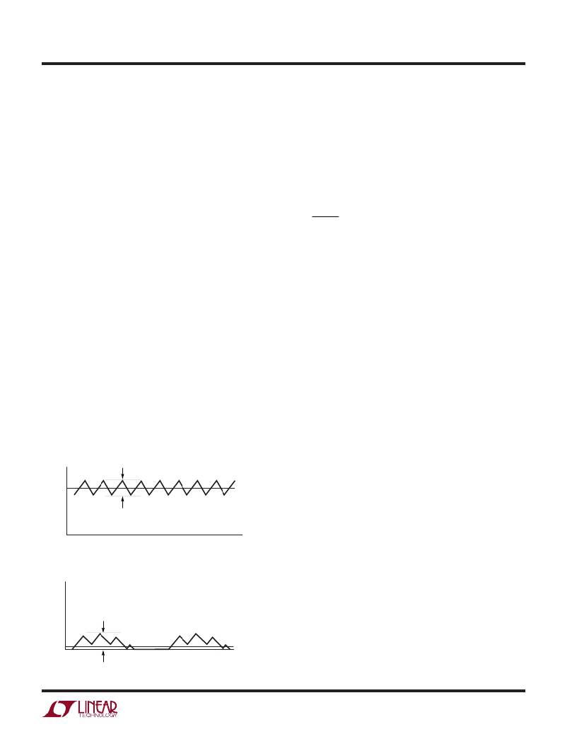
�Figure� 5a.� Continuous� Mode�
�I� RIPPLE�
�3802� F05a�
�back� loop� responds� and� requests� an� increase� in� duty� cycle.�
�During� sudden� transient� steps,� the� regulator� output� ripple�
�is� limited� by� the� feedback� loop� transient� response� and� is�
�independent� of� the� mode� of� operation.�
�The� small� 15mV� and� –12mV� offset� at� the� POS� and� NEG�
�RESET� comparators� ensure� that� after� a� transient� load� step,�
�the� LTC3802� returns� to� continuous� mode� quickly.� This�
�minimizes� the� output� ripple� under� Burst� Mode� operation.�
�TIME�
�Figure� 5b.� Burst� Mode� Operation�
�3802� F05b�
�I� AVERAGE�
�For� proper� Burst� Mode� operation,� the� LTC3802� requires�
�very� precise� CMPIN� and� FB� sensing.� To� realize� this,�
�CMPIN� and� FB� must� use� the� same� resistive� divider� values�
�3802f�
�19�
�相关PDF资料 |
PDF描述 |
|---|---|
| VI-J5K-EW-F4 | CONVERTER MOD DC/DC 40V 100W |
| H2BXG-10108-L4-ND | JUMPER-H1501TR/A2015L/X 8" |
| VI-J5K-EW-F3 | CONVERTER MOD DC/DC 40V 100W |
| LTC3731HG#TRPBF | IC REG CTRLR BUCK PWM CM 36-SSOP |
| VI-J5K-EW-F2 | CONVERTER MOD DC/DC 40V 100W |
相关代理商/技术参数 |
参数描述 |
|---|---|
| LTC3802EUH | 功能描述:IC REG CTRLR BUCK PWM VM 32-QFN RoHS:否 类别:集成电路 (IC) >> PMIC - 稳压器 - DC DC 切换控制器 系列:PolyPhase® 标准包装:4,500 系列:PowerWise® PWM 型:控制器 输出数:1 频率 - 最大:1MHz 占空比:95% 电源电压:2.8 V ~ 5.5 V 降压:是 升压:无 回扫:无 反相:无 倍增器:无 除法器:无 Cuk:无 隔离:无 工作温度:-40°C ~ 125°C 封装/外壳:6-WDFN 裸露焊盘 包装:带卷 (TR) 配用:LM1771EVAL-ND - BOARD EVALUATION LM1771 其它名称:LM1771SSDX |
| LTC3802EUH#PBF | 功能描述:IC REG CTRLR BUCK PWM VM 32-QFN RoHS:是 类别:集成电路 (IC) >> PMIC - 稳压器 - DC DC 切换控制器 系列:PolyPhase® 标准包装:4,500 系列:PowerWise® PWM 型:控制器 输出数:1 频率 - 最大:1MHz 占空比:95% 电源电压:2.8 V ~ 5.5 V 降压:是 升压:无 回扫:无 反相:无 倍增器:无 除法器:无 Cuk:无 隔离:无 工作温度:-40°C ~ 125°C 封装/外壳:6-WDFN 裸露焊盘 包装:带卷 (TR) 配用:LM1771EVAL-ND - BOARD EVALUATION LM1771 其它名称:LM1771SSDX |
| LTC3802EUH#TR | 功能描述:IC REG CTRLR BUCK PWM VM 32-QFN RoHS:否 类别:集成电路 (IC) >> PMIC - 稳压器 - DC DC 切换控制器 系列:PolyPhase® 标准包装:4,500 系列:PowerWise® PWM 型:控制器 输出数:1 频率 - 最大:1MHz 占空比:95% 电源电压:2.8 V ~ 5.5 V 降压:是 升压:无 回扫:无 反相:无 倍增器:无 除法器:无 Cuk:无 隔离:无 工作温度:-40°C ~ 125°C 封装/外壳:6-WDFN 裸露焊盘 包装:带卷 (TR) 配用:LM1771EVAL-ND - BOARD EVALUATION LM1771 其它名称:LM1771SSDX |
| LTC3802EUH#TRPBF | 功能描述:IC REG CTRLR BUCK PWM VM 32-QFN RoHS:是 类别:集成电路 (IC) >> PMIC - 稳压器 - DC DC 切换控制器 系列:PolyPhase® 标准包装:4,500 系列:PowerWise® PWM 型:控制器 输出数:1 频率 - 最大:1MHz 占空比:95% 电源电压:2.8 V ~ 5.5 V 降压:是 升压:无 回扫:无 反相:无 倍增器:无 除法器:无 Cuk:无 隔离:无 工作温度:-40°C ~ 125°C 封装/外壳:6-WDFN 裸露焊盘 包装:带卷 (TR) 配用:LM1771EVAL-ND - BOARD EVALUATION LM1771 其它名称:LM1771SSDX |
| LTC3803ES6 | 制造商:Linear Technology 功能描述:DC DC Cntrlr Single-OUT Flyback Controller 9.2V to 75V Input 6-Pin TSOT-23 |
发布紧急采购,3分钟左右您将得到回复。