- 您现在的位置:买卖IC网 > PDF目录15286 > LTC3810HUH-5#TRPBF (Linear Technology)IC REG CTRLR BUCK PWM CM 32-QFN PDF资料下载
参数资料
| 型号: | LTC3810HUH-5#TRPBF |
| 厂商: | Linear Technology |
| 文件页数: | 16/38页 |
| 文件大小: | 0K |
| 描述: | IC REG CTRLR BUCK PWM CM 32-QFN |
| 标准包装: | 2,500 |
| PWM 型: | 电流模式 |
| 输出数: | 1 |
| 频率 - 最大: | 1MHz |
| 占空比: | 99% |
| 电源电压: | 4.35 V ~ 60 V |
| 降压: | 是 |
| 升压: | 无 |
| 回扫: | 无 |
| 反相: | 无 |
| 倍增器: | 无 |
| 除法器: | 无 |
| Cuk: | 无 |
| 隔离: | 无 |
| 工作温度: | -40°C ~ 150°C |
| 封装/外壳: | 32-WFQFN 裸露焊盘 |
| 包装: | 带卷 (TR) |
第1页第2页第3页第4页第5页第6页第7页第8页第9页第10页第11页第12页第13页第14页第15页当前第16页第17页第18页第19页第20页第21页第22页第23页第24页第25页第26页第27页第28页第29页第30页第31页第32页第33页第34页第35页第36页第37页第38页
�� �
�
�LTC3810-5�
�APPLICATIONS� INFORMATION�
�V� OUT�
�V� IN�
�V� IN� –� V� OUT�
�V� IN�
�(� I� MAX� )� 2� (� ρ� T� )R� DS(ON)� +�
�P� TOP� =�
�V�
�+� V�
�–�
�V� IN2� MAX� (R� DR� )(C� MILLER� )� ?�
�1�
�1�
�?� ?� V� CC� –� V� TH(IL)�
�V� TH(IL)� ?� ?�
�(I� MAX� )� 2� (� ρ� T� )R� DS(0N)�
�P� BOT� =� IN�
�Themostimportantparameterinhighvoltageapplications�
�is� breakdown� voltage� BV� DSS� .� Both� the� top� and� bottom�
�MOSFETs� will� see� full� input� voltage� plus� any� additional�
�ringing� on� the� switch� node� across� its� drain-to-source� dur-�
�ing� its� off-time� and� must� be� chosen� with� the� appropriate�
�breakdown� specification.� The� LTC3810-5� is� designed� to�
�be� used� with� a� 4.5V� to� 14V� gate� drive� supply� (DRV� CC� pin)�
�for� driving� logic-level� MOSFETs� (V� GS(MIN)� ≥� 4.5V).�
�For� maximum� efficiency,� on-resistance� R� DS(ON)� and� input�
�capacitance� should� be� minimized.� Low� R� DS(ON)� minimizes�
�conduction� losses� and� low� input� capacitance� minimizes�
�transition� losses.� MOSFET� input� capacitance� is� a� combi-�
�nation� of� several� components� but� can� be� taken� from� the�
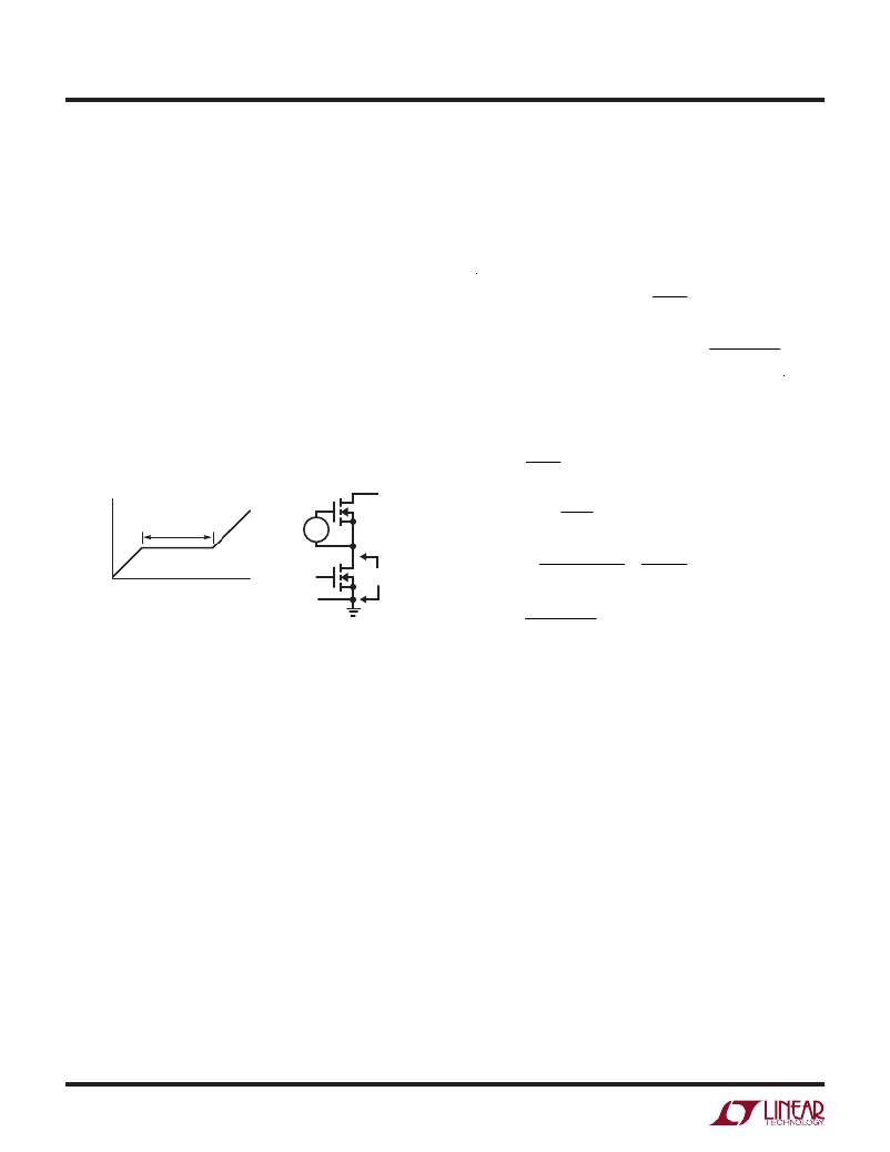
�typical� “gate� charge”� curve� included� on� most� data� sheets�
�(Figure� 6).�
�V� IN�
�MILLER� EFFECT�
�V� GS�
�a� b�
�+� DS�
�Q� IN� V� GS�
�C� MILLER� =� (Q� B� –� Q� A� )/V� DS� –�
�38105� F06�
�Figure� 6.� Gate� Charge� Characteristic�
�The� curve� is� generated� by� forcing� a� constant� input� cur-�
�rent� into� the� gate� of� a� common� source,� current� source�
�loaded� stage� and� then� plotting� the� gate� voltage� versus�
�time.� The� initial� slope� is� the� effect� of� the� gate-to-source�
�and� the� gate-to-drain� capacitance.� The� flat� portion� of� the�
�curve� is� the� result� of� the� Miller� multiplication� effect� of� the�
�drain-to-gate� capacitance� as� the� drain� drops� the� voltage�
�across� the� current� source� load.� The� upper� sloping� line� is�
�due� to� the� drain-to-gate� accumulation� capacitance� and�
�the� gate-to-source� capacitance.� The� Miller� charge� (the�
�increase� in� coulombs� on� the� horizontal� axis� from� a� to� b�
�while� the� curve� is� flat)� is� specified� for� a� given� V� DS� drain�
�voltage,� but� can� be� adjusted� for� different� V� DS� voltages� by�
�multiplying� by� the� ratio� of� the� application� V� DS� to� the� curve�
�specified� V� DS� values.� A� way� to� estimate� the� C� MILLER� term�
�is� to� take� the� change� in� gate� charge� from� points� a� and� b�
�on� a� manufacturers� data� sheet� and� divide� by� the� stated�
�V� DS� voltage� specified.� C� MILLER� is� the� most� important� se-�
�lection� criteria� for� determining� the� transition� loss� term� in�
�the� top� MOSFET� but� is� not� directly� specified� on� MOSFET�
�data� sheets.� C� RSS� and� C� OS� are� specified� sometimes� but�
�definitions� of� these� parameters� are� not� included.�
�When� the� controller� is� operating� in� continuous� mode� the�
�duty� cycles� for� the� top� and� bottom� MOSFETs� are� given� by:�
�Main� Switch� Duty� Cycle� =�
�Synchronous� Switch� Duty� Cycle� =�
�The� power� dissipation� for� the� main� and� synchronous�
�MOSFETs� at� maximum� output� current� are� given� by:�
�V� OUT�
�V� IN�
�I�
�2�
�?� ?�
�?� +� ?� (f)�
�V – V� OUT�
�V� IN�
�where� ρ� T� is� the� temperature� dependency� of� R� DS(ON)� ,� R� DR�
�is� the� effective� top� driver� resistance� (approximately� 2Ω� at�
�V� GS� =� V� MILLER� ),� V� IN� is� the� drain� potential� and� the� change�
�in� drain� potential� in� the� particular� application.� V� TH(IL)� is�
�the� data� sheet� specified� typical� gate� threshold� voltage�
�specified� in� the� power� MOSFET� data� sheet� at� the� specified�
�drain� current.� C� MILLER� is� the� calculated� capacitance� using�
�the� gate� charge� curve� from� the� MOSFET� data� sheet� and�
�the� technique� described� above.�
�Both� MOSFETs� have� I� 2� R� losses� while� the� topside� N-channel�
�equation� incudes� an� additional� term� for� transition� losses,�
�which� peak� at� the� highest� input� voltage.� For� high� input�
�voltage� low� duty� cycle� applications� that� are� typical� for� the�
�LTC3810-5,� transition� losses� are� the� dominate� loss� term� and�
�therefore� using� higher� R� DS(ON)� device� with� lower� C� MILLER�
�usually� provides� the� highest� efficiency.� The� synchronous�
�MOSFET� losses� are� greatest� at� high� input� voltage� when�
�the� top� switch� duty� factor� is� low� or� during� a� short-circuit�
�when� the� synchronous� switch� is� on� close� to� 100%� of�
�38105fd�
�16�
�相关PDF资料 |
PDF描述 |
|---|---|
| LTC3834EUFD#TRPBF | IC REG CTRLR BUCK PWM CM 20-QFN |
| LTC3834EFE#TRPBF | IC REG CTRLR BUCK PWM CM 20TSSOP |
| VI-B2Z-EY-F2 | CONVERTER MOD DC/DC 2V 20W |
| LTC1148CS | IC REG CTRLR BUCK PWM CM 14-SOIC |
| VI-B2Z-EY-F1 | CONVERTER MOD DC/DC 2V 20W |
相关代理商/技术参数 |
参数描述 |
|---|---|
| LTC3810IG | 制造商:Linear Technology 功能描述: |
| LTC3810IG#PBF | 功能描述:IC REG CTRLR BUCK PWM CM 28-SSOP RoHS:是 类别:集成电路 (IC) >> PMIC - 稳压器 - DC DC 切换控制器 系列:- 标准包装:2,500 系列:- PWM 型:电流模式 输出数:1 频率 - 最大:500kHz 占空比:96% 电源电压:4 V ~ 36 V 降压:无 升压:是 回扫:无 反相:无 倍增器:无 除法器:无 Cuk:无 隔离:无 工作温度:-40°C ~ 125°C 封装/外壳:24-WQFN 裸露焊盘 包装:带卷 (TR) |
| LTC3810IG#TRPBF | 功能描述:IC REG CTRLR BUCK PWM CM 28-SSOP RoHS:是 类别:集成电路 (IC) >> PMIC - 稳压器 - DC DC 切换控制器 系列:- 标准包装:2,500 系列:- PWM 型:电流模式 输出数:1 频率 - 最大:500kHz 占空比:96% 电源电压:4 V ~ 36 V 降压:无 升压:是 回扫:无 反相:无 倍增器:无 除法器:无 Cuk:无 隔离:无 工作温度:-40°C ~ 125°C 封装/外壳:24-WQFN 裸露焊盘 包装:带卷 (TR) |
| LTC3810IUH-5#PBF | 功能描述:IC REG CTRLR BUCK PWM CM 32-QFN RoHS:是 类别:集成电路 (IC) >> PMIC - 稳压器 - DC DC 切换控制器 系列:- 标准包装:2,500 系列:- PWM 型:电流模式 输出数:1 频率 - 最大:500kHz 占空比:96% 电源电压:4 V ~ 36 V 降压:无 升压:是 回扫:无 反相:无 倍增器:无 除法器:无 Cuk:无 隔离:无 工作温度:-40°C ~ 125°C 封装/外壳:24-WQFN 裸露焊盘 包装:带卷 (TR) |
| LTC3810IUH-5#TRPBF | 功能描述:IC REG CTRLR BUCK PWM CM 32-QFN RoHS:是 类别:集成电路 (IC) >> PMIC - 稳压器 - DC DC 切换控制器 系列:- 标准包装:2,500 系列:- PWM 型:电流模式 输出数:1 频率 - 最大:500kHz 占空比:96% 电源电压:4 V ~ 36 V 降压:无 升压:是 回扫:无 反相:无 倍增器:无 除法器:无 Cuk:无 隔离:无 工作温度:-40°C ~ 125°C 封装/外壳:24-WQFN 裸露焊盘 包装:带卷 (TR) |
发布紧急采购,3分钟左右您将得到回复。