- 您现在的位置:买卖IC网 > PDF目录1832 > LTC3811EUHF#TRPBF (Linear Technology)IC REG CTRLR BUCK PWM CM 38-QFN PDF资料下载
参数资料
| 型号: | LTC3811EUHF#TRPBF |
| 厂商: | Linear Technology |
| 文件页数: | 16/48页 |
| 文件大小: | 0K |
| 描述: | IC REG CTRLR BUCK PWM CM 38-QFN |
| 标准包装: | 2,500 |
| 系列: | PolyPhase® |
| PWM 型: | 电流模式 |
| 输出数: | 2 |
| 频率 - 最大: | 850kHz |
| 占空比: | 90% |
| 电源电压: | 4.5 V ~ 30 V |
| 降压: | 是 |
| 升压: | 无 |
| 回扫: | 无 |
| 反相: | 无 |
| 倍增器: | 无 |
| 除法器: | 无 |
| Cuk: | 无 |
| 隔离: | 无 |
| 工作温度: | -40°C ~ 85°C |
| 封装/外壳: | 38-WFQFN 裸露焊盘 |
| 包装: | 带卷 (TR) |
第1页第2页第3页第4页第5页第6页第7页第8页第9页第10页第11页第12页第13页第14页第15页当前第16页第17页第18页第19页第20页第21页第22页第23页第24页第25页第26页第27页第28页第29页第30页第31页第32页第33页第34页第35页第36页第37页第38页第39页第40页第41页第42页第43页第44页第45页第46页第47页第48页
�� �
�
�LTC3811�
�OPERATION�
�(Refer� to� the� Functional� Diagram)�
�be� increased� to� 10μF.� Because� of� the� high� peak� current�
�capability� of� the� gate� driver,� it� is� essential� that� this� capacitor�
�be� placed� as� close� as� possible� to� DRV� CC� and� PGND� pins,�
�and� on� the� same� PCB� layer� as� the� IC.�
�The� INTV� CC� pin� supplies� power� to� all� of� the� low� voltage�
�analog� circuitry� and� is� electrically� isolated� from� DRV� CC� .� The�
�INTV� CC� supply� is� normally� derived� from� DRV� CC� through�
�an� RC� ?lter,� in� order� to� prevent� gate� driver� supply� noise�
�from� coupling� into� sensitive� analog� control� circuitry.� Typi-�
�cal� values� for� this� RC� ?lter� consist� of� a� 1� Ω� resistor� from�
�DRV� CC� to� INTV� CC� and� a� 0.1μF� low� ESR� ceramic� capacitor�
�from� INTV� CC� to� SGND.� The� INTV� CC� capacitor� should� be�
�placed� as� close� as� possible� to� the� INTV� CC� and� SGND� pins�
�and� on� the� same� PCB� layer� as� the� IC.�
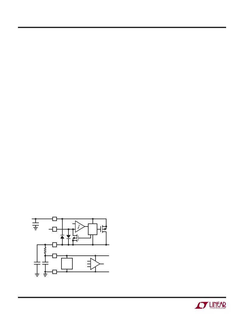
�A� third� power� supply� pin,� EXTV� CC� ,� serves� as� an� auxiliary�
�input� for� applications� where� the� power� dissipation� in� the�
�internal� LDO� is� excessive,� or� where� maximum� ef?ciency�
�is� essential.� This� con?guration� is� shown� in� Figure� 2.� When�
�the� EXTV� CC� pin� is� left� open� or� is� connected� to� a� voltage�
�less� than� 4.5V,� the� internal� 6V� LDO� supplies� DRV� CC� power�
�from� V� IN� .� If� EXTV� CC� is� tied� to� an� external� power� supply�
�greater� than� 4.5V,� however,� the� 6V� LDO� is� turned� off� and�
�power� is� supplied� to� DRV� CC� through� a� 5� Ω� PMOS� switch�
�from� EXTV� CC� .� For� 4.5V� <� EXTV� CC� <� 7V� this� PMOS� switch�
�is� on� and� DRV� CC� is� approximately� equal� to� EXTV� CC� .� Using�
�the� EXTV� CC� pin� allows� the� gate� driver� and� control� power� to�
�be� derived� from� a� high� ef?ciency� external� source,� dramati-�
�cally� reducing� power� dissipation� on� the� IC.�
�Using� an� External� 5V� Supply� to� Measure� Dynamic�
�Quiescent� Current�
�When� a� voltage� above� 4.5V� is� applied� to� the� EXTV� CC� pin,� the�
�internal� LDO� in� the� LTC3811� is� switched� off� and� the� power�
�is� supplied� by� the� external� 5V� power� supply� as� shown� in�
�Figure� 2.� Under� these� conditions,� the� quiescent� current�
�at� the� V� IN� pin� of� the� IC� is� very� low� (less� than� 1mA),� and�
�most� of� the� current� required� to� power� the� analog� control�
�circuitry� and� the� gate� drivers� ?ows� into� the� EXTV� CC� pin.� As�
�a� result,� this� auxiliary� supply� can� be� used� as� a� diagnostic�
�tool� in� order� to� measure� the� total� current� for� thermal�
�calculations.� In� order� to� match� the� actual� condition� when�
�the� internal� LDO� is� on,� the� voltage� applied� to� EXTV� CC� when�
�the� measurements� are� taken� should� be� 6V� (the� same� as�
�the� regulated� LDO� output� voltage).�
�Once� the� total� quiescent� current� for� the� application� is�
�known,� the� power� dissipation,� P� D� ,� on� the� IC� will� be� ap-�
�proximately� I� EXTVCC� times� V� IN� ,� since� the� gate� drive� current�
�and� control� circuitry� quiescent� current� would� be� required�
�to� ?ow� through� the� V� IN� pin.� The� junction� temperature� of�
�the� IC� can� then� be� estimated� using� the� following� well-�
�known� formula:�
�T� J� =� T� A� +� (P� D� ?� R� θ� JA� )�
�If� the� maximum� junction� temperature� is� close� to� the� Abso-�
�lute� Maximum� Rating� for� the� particular� device� being� used,�
�the� use� of� an� auxiliary� supply� and� the� EXTV� CC� pin� may� be�
�required.� Alternatively,� lower� gate� charge� MOSFETs� should�
�be� used� or� the� switching� frequency� should� be� reduced.�
�V� IN�
�V� IN�
�Operation� at� Low� Supply� Voltage�
�AUX� 5V�
�SUPPLY�
�EXTV� CC�
�4.5V�
�+�
�–�
�6V�
�LDO�
�The� LTC3811� control� circuit� has� a� minimum� input� volt-�
�age� of� 4.5V,� making� it� a� good� choice� for� applications� that�
�experience� low� supply� conditions.� However,� care� should�
�DRV� CC�
�GATE� DRIVER� SUPPLY�
�be� taken� to� determine� the� minimum� gate� drive� supply�
�voltage� in� order� to� choose� the� optimum� power� MOSFETs.�
�INTV� CC�
�ANALOG� SUPPLY�
�Important� parameters� that� can� affect� the� minimum� gate�
�SGND�
�BIAS�
�V� FB�
�SS/TRACK�
�0.600V�
�EA�
�drive� voltage� are� the� minimum� input� voltage� (V� IN� ),� the�
�LDO� dropout� voltage,� and� the� EXTV� CC� supply� voltage,� if�
�an� external� gate� drive� supply� is� being� used.�
�3811� F02�
�Figure� 2.� Supplying� Power� to� the� LTC3811� from� EXTV� CC�
�3811f�
�16�
�相关PDF资料 |
PDF描述 |
|---|---|
| LTC3812EFE-5#PBF | IC REG CTRLR BUCK PWM CM 16TSSOP |
| LTC3813EG#PBF | IC REG CTRLR BST PWM CM 28-SSOP |
| LTC3814EFE-5#PBF | IC REG CTRLR BST PWM CM 16-TSSOP |
| LTC3816IFE#TRPBF | IC CONTROLLER S-PHASE 38TSSOP |
| LTC3819EG#TRPBF | IC CNTRLR STEP DOWN 36-SSOP |
相关代理商/技术参数 |
参数描述 |
|---|---|
| LTC3812EFE5#PBF | 制造商:Linear Technology 功能描述: |
| LTC3812EFE-5#PBF | 功能描述:IC REG CTRLR BUCK PWM CM 16TSSOP RoHS:是 类别:集成电路 (IC) >> PMIC - 稳压器 - DC DC 切换控制器 系列:- 特色产品:LM3753/54 Scalable 2-Phase Synchronous Buck Controllers 标准包装:1 系列:PowerWise® PWM 型:电压模式 输出数:1 频率 - 最大:1MHz 占空比:81% 电源电压:4.5 V ~ 18 V 降压:是 升压:无 回扫:无 反相:无 倍增器:无 除法器:无 Cuk:无 隔离:无 工作温度:-5°C ~ 125°C 封装/外壳:32-WFQFN 裸露焊盘 包装:Digi-Reel® 产品目录页面:1303 (CN2011-ZH PDF) 其它名称:LM3754SQDKR |
| LTC3812EFE-5#TRPBF | 功能描述:IC REG CTRLR BUCK PWM CM 16TSSOP RoHS:是 类别:集成电路 (IC) >> PMIC - 稳压器 - DC DC 切换控制器 系列:- 标准包装:2,500 系列:- PWM 型:电流模式 输出数:1 频率 - 最大:500kHz 占空比:96% 电源电压:4 V ~ 36 V 降压:无 升压:是 回扫:无 反相:无 倍增器:无 除法器:无 Cuk:无 隔离:无 工作温度:-40°C ~ 125°C 封装/外壳:24-WQFN 裸露焊盘 包装:带卷 (TR) |
| LTC3812IFE-5#PBF | 功能描述:IC REG CTRLR BUCK PWM CM 16TSSOP RoHS:是 类别:集成电路 (IC) >> PMIC - 稳压器 - DC DC 切换控制器 系列:- 标准包装:2,500 系列:- PWM 型:电流模式 输出数:1 频率 - 最大:500kHz 占空比:96% 电源电压:4 V ~ 36 V 降压:无 升压:是 回扫:无 反相:无 倍增器:无 除法器:无 Cuk:无 隔离:无 工作温度:-40°C ~ 125°C 封装/外壳:24-WQFN 裸露焊盘 包装:带卷 (TR) |
| LTC3812IFE-5#TRPBF | 功能描述:IC REG CTRLR BUCK PWM CM 16TSSOP RoHS:是 类别:集成电路 (IC) >> PMIC - 稳压器 - DC DC 切换控制器 系列:- 标准包装:2,500 系列:- PWM 型:电流模式 输出数:1 频率 - 最大:500kHz 占空比:96% 电源电压:4 V ~ 36 V 降压:无 升压:是 回扫:无 反相:无 倍增器:无 除法器:无 Cuk:无 隔离:无 工作温度:-40°C ~ 125°C 封装/外壳:24-WQFN 裸露焊盘 包装:带卷 (TR) |
发布紧急采购,3分钟左右您将得到回复。