- 您现在的位置:买卖IC网 > PDF目录15349 > LTC3822EMSE#PBF (Linear Technology)IC REG CTRLR BUCK PWM CM 10-MSOP PDF资料下载
参数资料
| 型号: | LTC3822EMSE#PBF |
| 厂商: | Linear Technology |
| 文件页数: | 14/20页 |
| 文件大小: | 0K |
| 描述: | IC REG CTRLR BUCK PWM CM 10-MSOP |
| 标准包装: | 50 |
| PWM 型: | 电流模式 |
| 输出数: | 1 |
| 频率 - 最大: | 850kHz |
| 占空比: | 99% |
| 电源电压: | 2.75 V ~ 4.5 V |
| 降压: | 是 |
| 升压: | 无 |
| 回扫: | 无 |
| 反相: | 无 |
| 倍增器: | 无 |
| 除法器: | 无 |
| Cuk: | 无 |
| 隔离: | 无 |
| 工作温度: | -40°C ~ 85°C |
| 封装/外壳: | 10-TFSOP,10-MSOP(0.118",3.00mm 宽)裸露焊盘 |
| 包装: | 管件 |
| 产品目录页面: | 1336 (CN2011-ZH PDF) |
�� �
�
�LTC3822�
�APPLICATIONS� INFORMATION�
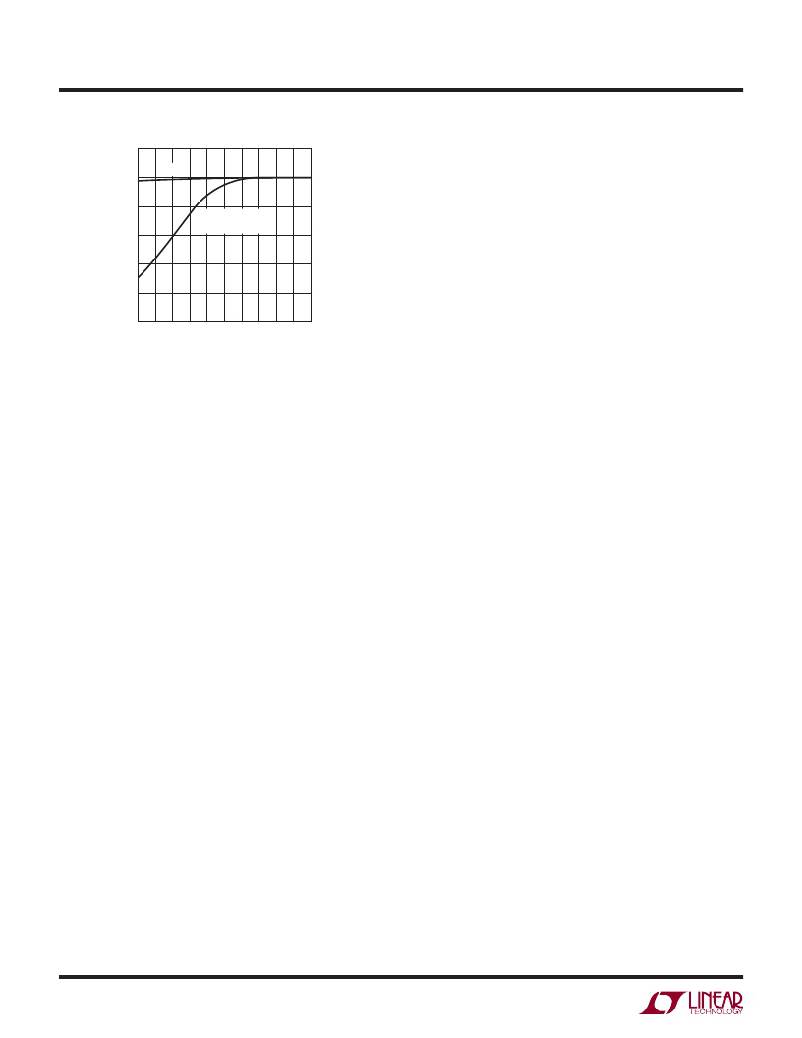
�105�
�3)� I� 2� R� losses� are� calculated� from� the� DC� resistances� of� the�
�100�
�95�
�90�
�85�
�80�
�75�
�V� REF�
�MAXIMUM�
�SENSE� VOLTAGE�
�2.0� 2.1� 2.2� 2.3� 2.4� 2.5� 2.6� 2.7� 2.8� 2.9� 3.0�
�MOSFETs,� inductor� and/or� sense� resistor.� In� continuous�
�mode,� the� average� output� current� ?ows� through� L� but�
�is� “chopped”� between� the� top� MOSFET� and� the� bottom�
�MOSFET.� Each� MOSFET’s� R� DS(ON)� can� be� multiplied� by� its�
�respective� duty� cycle� and� summed� together� with� the� DCR�
�of� the� inductor� to� obtain� I� 2� R� losses.�
�4)� Transition� losses� apply� to� the� external� MOSFET� and�
�increase� with� higher� operating� frequencies� and� input�
�voltages.� Transition� losses� can� be� estimated� from:�
�INPUT� VOLTAGE� (V)�
�3822� F04�
�Transition� Loss� =� 2� ?� V� IN2� ?� I� O(MAX)� ?� C� RSS� ?� f�
�Figure� 4.� Line� Regulation� of� V� REF� and� Maximum� Sense� Voltage�
�Ef?ciency� Considerations�
�The� ef?ciency� of� a� switching� regulator� is� equal� to� the�
�output� power� divided� by� the� input� power.� It� is� often� useful�
�to� analyze� individual� losses� to� determine� what� is� limiting�
�ef?ciency� and� which� change� would� produce� the� most�
�improvement.� Ef?ciency� can� be� expressed� as:�
�Ef?ciency� =� 100%� –� (L1� +� L2� +� L3� +� …)�
�where� L1,� L2,� etc.� are� the� individual� losses� as� a� percent-�
�age� of� input� power.�
�Although� all� dissipative� elements� in� the� circuit� produce�
�losses,� four� main� sources� usually� account� for� most� of�
�the� losses� in� LTC3822� circuits:� 1)� LTC3822� DC� bias� cur-�
�rent,� 2)� MOSFET� gate� charge� current,� 3)� I� 2� R� losses� and�
�4)� transition� losses.�
�1)� The� V� IN� (pin)� current� is� the� DC� supply� current,� given�
�in� the� Electrical� Characteristics,� which� excludes� MOSFET�
�driver� currents.� V� IN� current� results� in� a� small� loss� that�
�increases� with� V� IN� .�
�2)� MOSFET� gate� charge� current� results� from� switching�
�the� gate� capacitance� of� the� power� MOSFET.� Each� time� a�
�MOSFET� gate� is� switched� from� low� to� high� to� low� again,�
�a� packet� of� charge� dQ� moves� from� BOOST� to� ground.� The�
�resulting� dQ/dt� is� a� current� out� of� BOOST,� which� is� typically�
�much� larger� than� the� V� IN� supply� current.� In� continuous�
�mode,� I� GATECHG� =� f� ?� Q� P� .�
�Other� losses,� including� C� IN� and� C� OUT� ESR� dissipative� losses�
�and� inductor� core� losses,� generally� account� for� less� than�
�2%� total� additional� loss.�
�Checking� Transient� Response�
�The� regulator� loop� response� can� be� checked� by� looking�
�at� the� load� transient� response.� Switching� regulators� take�
�several� cycles� to� respond� to� a� step� in� load� current.� When�
�a� load� step� occurs,� V� OUT� immediately� shifts� by� an� amount�
�equal� to� (� Δ� I� LOAD� )� ?� (ESR),� where� ESR� is� the� effective� se-�
�ries� resistance� of� C� OUT� .� Δ� I� LOAD� also� begins� to� charge� or�
�discharge� C� OUT� generating� a� feedback� error� signal� used�
�by� the� regulator� to� return� V� OUT� to� its� steady-state� value.�
�During� this� recovery� time,� V� OUT� can� be� monitored� for�
�overshoot� or� ringing� that� would� indicate� a� stability� problem.�
�OPTI-LOOP� compensation� allows� the� transient� response�
�to� be� optimized� over� a� wide� range� of� output� capacitance�
�and� ESR� values.�
�The� I� TH� series� R� C� -C� C� ?lter� (see� the� Functional� Diagram)�
�sets� the� dominant� pole-zero� loop� compensation.�
�The� I� TH� external� components� showed� in� the� ?gure� on� the�
�?rst� page� of� this� data� sheet� will� provide� adequate� compen-�
�sation� for� most� applications.� The� values� can� be� modi?ed�
�slightly� (from� 0.2� to� 5� times� their� suggested� values)� to�
�optimize� transient� response� once� the� ?nal� PC� layout� is� done�
�and� the� particular� output� capacitor� type� and� value� have�
�been� determined.� The� output� capacitor� needs� to� be� decided�
�upon� because� the� various� types� and� values� determine� the�
�loop� feedback� factor� gain� and� phase.� An� output� current�
�pulse� of� 20%� to� 100%� of� full� load� current� having� a� rise�
�time� of� 1μs� to� 10μs� will� produce� output� voltage� and� I� TH�
�3822fa�
�14�
�相关PDF资料 |
PDF描述 |
|---|---|
| H2BBT-10104-V8-ND | JUMPER-H1500TR/A3048V/H1500TR 4" |
| LTC1622CS8 | IC REG CTRLR BUCK PWM CM 8-SOIC |
| H2BBT-10104-S8-ND | JUMPER-H1500TR/A3048S/H1500TR 4" |
| MIC2159YMME TR | IC REG CTRLR BUCK PWM VM 10-MSOP |
| H2BBT-10104-R8-ND | JUMPER-H1500TR/A3048R/H1500TR 4" |
相关代理商/技术参数 |
参数描述 |
|---|---|
| LTC3823EGN#PBF | 功能描述:IC REG CTRLR BUCK PWM CM 28-SSOP RoHS:是 类别:集成电路 (IC) >> PMIC - 稳压器 - DC DC 切换控制器 系列:- 标准包装:2,500 系列:- PWM 型:电流模式 输出数:1 频率 - 最大:500kHz 占空比:96% 电源电压:4 V ~ 36 V 降压:无 升压:是 回扫:无 反相:无 倍增器:无 除法器:无 Cuk:无 隔离:无 工作温度:-40°C ~ 125°C 封装/外壳:24-WQFN 裸露焊盘 包装:带卷 (TR) |
| LTC3823EGN#TRPBF | 功能描述:IC REG CTRLR BUCK PWM CM 28-SSOP RoHS:是 类别:集成电路 (IC) >> PMIC - 稳压器 - DC DC 切换控制器 系列:- 标准包装:2,500 系列:- PWM 型:电流模式 输出数:1 频率 - 最大:500kHz 占空比:96% 电源电压:4 V ~ 36 V 降压:无 升压:是 回扫:无 反相:无 倍增器:无 除法器:无 Cuk:无 隔离:无 工作温度:-40°C ~ 125°C 封装/外壳:24-WQFN 裸露焊盘 包装:带卷 (TR) |
| LTC3823EUH#PBF | 功能描述:IC REG CTRLR BUCK PWM CM 32-QFN RoHS:是 类别:集成电路 (IC) >> PMIC - 稳压器 - DC DC 切换控制器 系列:- 标准包装:2,000 系列:- PWM 型:电流模式 输出数:1 频率 - 最大:1MHz 占空比:50% 电源电压:9 V ~ 10 V 降压:无 升压:是 回扫:是 反相:无 倍增器:无 除法器:无 Cuk:无 隔离:无 工作温度:-40°C ~ 85°C 封装/外壳:8-TSSOP(0.173",4.40mm 宽) 包装:带卷 (TR) |
| LTC3823EUH#TRPBF | 功能描述:IC REG CTRLR BUCK PWM CM 32-QFN RoHS:是 类别:集成电路 (IC) >> PMIC - 稳压器 - DC DC 切换控制器 系列:- 标准包装:2,500 系列:- PWM 型:电流模式 输出数:1 频率 - 最大:500kHz 占空比:96% 电源电压:4 V ~ 36 V 降压:无 升压:是 回扫:无 反相:无 倍增器:无 除法器:无 Cuk:无 隔离:无 工作温度:-40°C ~ 125°C 封装/外壳:24-WQFN 裸露焊盘 包装:带卷 (TR) |
| LTC3823IGN#PBF | 功能描述:IC REG CTRLR BUCK PWM CM 28-SSOP RoHS:是 类别:集成电路 (IC) >> PMIC - 稳压器 - DC DC 切换控制器 系列:- 标准包装:2,000 系列:- PWM 型:电流模式 输出数:1 频率 - 最大:1MHz 占空比:50% 电源电压:9 V ~ 10 V 降压:无 升压:是 回扫:是 反相:无 倍增器:无 除法器:无 Cuk:无 隔离:无 工作温度:-40°C ~ 85°C 封装/外壳:8-TSSOP(0.173",4.40mm 宽) 包装:带卷 (TR) |
发布紧急采购,3分钟左右您将得到回复。