- 您现在的位置:买卖IC网 > PDF目录15503 > LTC3830ES#PBF (Linear Technology)IC REG CTRLR BUCK PWM VM 16-SOIC PDF资料下载
参数资料
| 型号: | LTC3830ES#PBF |
| 厂商: | Linear Technology |
| 文件页数: | 3/24页 |
| 文件大小: | 0K |
| 描述: | IC REG CTRLR BUCK PWM VM 16-SOIC |
| 标准包装: | 50 |
| PWM 型: | 电压模式 |
| 输出数: | 1 |
| 频率 - 最大: | 250kHz |
| 占空比: | 95% |
| 电源电压: | 3 V ~ 8 V |
| 降压: | 是 |
| 升压: | 无 |
| 回扫: | 无 |
| 反相: | 无 |
| 倍增器: | 无 |
| 除法器: | 无 |
| Cuk: | 无 |
| 隔离: | 无 |
| 工作温度: | -40°C ~ 85°C |
| 封装/外壳: | 16-SOIC(0.154",3.90mm 宽) |
| 包装: | 管件 |
| 产品目录页面: | 1336 (CN2011-ZH PDF) |
�� �
�
�LTC3830/LTC3830-1�
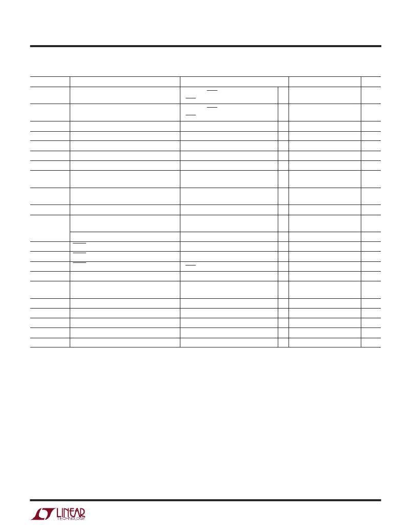
�ELECTRICAL� CHARACTERISTICS�
�The� ●� denotes� specifications� that� apply� over� the� full� operating� temperature�
�range,� otherwise� specifications� are� at� T� A� =� 25� °� C.� V� CC� ,� PV� CC1� ,� PV� CC2� =� 5V,� unless� otherwise� noted.� (Note� 2)�
�SYMBOL�
�I� VCC�
�I� PVCC�
�PARAMETER�
�Supply� Current�
�PV� CC� Supply� Current�
�CONDITIONS�
�Figure� 2,� V� SHDN� =� V� CC�
�V� SHDN� =� 0V�
�Figure� 2,� V� SHDN� =� V� CC� (Note� 3)�
�V� SHDN� =� 0V�
�●�
�●�
�●�
�●�
�MIN�
�TYP�
�0.7�
�1�
�14�
�0.1�
�MAX�
�1.6�
�10�
�20�
�10�
�UNITS�
�mA�
�μ� A�
�mA�
�μ� A�
�f� OSC�
�Internal� Oscillator� Frequency�
�FREQSET� Floating�
�●�
�160�
�200�
�250�
�kHz�
�V� SAWL�
�V� SAWH�
�V� COMP� at� Minimum� Duty� Cycle�
�V� COMP� at� Maximum� Duty� Cycle�
�1.2�
�2.2�
�V�
�V�
�V� COMPMAX�
�Maximum� V� COMP�
�V� FB� =� 0V,� PV� CC1� =� 8V�
�2.85�
�V�
�?� f� OSC� /� ?� I� FREQSET� Frequency� Adjustment�
�10�
�kHz/� μ� A�
�A� V�
�Error� Amplifier� Open-Loop� DC� Gain�
�Measured� from� FB� to� COMP,�
�SENSE� +� and� SENSE� –� Floating,� (Note� 4)�
�●�
�46�
�55�
�dB�
�g� m�
�Error� Amplifier� Transconductance�
�Measured� from� FB� to� COMP,�
�SENSE� +� and� SENSE� –� Floating,� (Note� 4)�
�●�
�520�
�650�
�780�
�μ� mho�
�I� COMP�
�Error� Amplifier� Output� Sink/Source� Current�
�100�
�μ� A�
�I� MAX�
�I� MAX� Sink� Current�
�V� IMAX� =� V� CC�
�(Note� 10)�
�●�
�9�
�4�
�12�
�12�
�15�
�20�
�μ� A�
�μ� A�
�I� MAX� Sink� Current� Tempco�
�V� IMAX� =� V� CC� (Note� 6)�
�3300�
�ppm/� °� C�
�V� IH�
�V� IL�
�SHDN� Input� High� Voltage�
�SHDN� Input� Low� Voltage�
�●�
�●�
�2.4�
�0.8�
�V�
�V�
�I� IN�
�SHDN� Input� Current�
�V� SHDN� =� V� CC�
�●�
�0.1�
�1�
�μ� A�
�I� SS�
�Soft-Start� Source� Current�
�V� SS� =� 0V,� V� IMAX� =� 0V,� V� IFB� =� V� CC�
�●�
�–8�
�–12�
�–16�
�μ� A�
�I� SSIL�
�Maximum� Soft-Start� Sink� Current�
�V� IMAX� =� V� CC� ,� V� IFB� =� 0V,�
�1.6�
�mA�
�In� Current� Limit�
�V� SS� =� V� CC� (Note� 8),� PV� CC1� =� 8V�
�R� SENSE�
�R� SENSEFB�
�SENSE� Input� Resistance�
�SENSE� to� FB� Resistance�
�29.2�
�18�
�k� ?�
�k� ?�
�t� r� ,� t� f�
�Driver� Rise/Fall� Time�
�Figure� 3,� PV� CC1� =� PV� CC2� =� 5V� (Note� 5)�
�●�
�80�
�250�
�ns�
�t� NOV�
�DC� MAX�
�Driver� Nonoverlap� Time�
�Maximum� G1� Duty� Cycle�
�Figure� 3,� PV� CC1� =� PV� CC2� =� 5V� (Note� 5)�
�Figure� 3,� V� FB� =� 0V� (Note� 5),� PV� CC1� =� 8V�
�●�
�●�
�25�
�91�
�120�
�95�
�250�
�ns�
�%�
�Note� 1:� Absolute� Maximum� Ratings� are� those� values� beyond� which� the� life�
�of� a� device� may� be� impaired.�
�Note� 2:� All� currents� into� device� pins� are� positive;� all� currents� out� of� device�
�pins� are� negative.� All� voltages� are� referenced� to� ground� unless� otherwise�
�specified.�
�Note� 3:� Supply� current� in� normal� operation� is� dominated� by� the� current�
�needed� to� charge� and� discharge� the� external� FET� gates.� This� will� vary� with�
�the� LTC3830� operating� frequency,� operating� voltage� and� the� external� FETs�
�used.�
�Note� 4:� The� open-loop� DC� gain� and� transconductance� from� the� SENSE� +�
�and� SENSE� –� pins� to� COMP� pin� will� be� (A� V� )(1.265/3.3)� and� (g� m� )(1.265/3.3)�
�respectively.�
�Note� 5:� Rise� and� fall� times� are� measured� using� 10%� and� 90%� levels.� Duty�
�cycle� and� nonoverlap� times� are� measured� using� 50%� levels.�
�Note� 6:� Guaranteed� by� design,� not� subject� to� test.�
�Note� 7:� PV� CC1� must� be� higher� than� V� CC� by� at� least� 2.5V� for� G1� to� operate�
�at� 95%� maximum� duty� cycle� and� for� the� current� limit� protection� circuit� to�
�Note� 8:� The� current� limiting� amplifier� can� sink� but� cannot� source� current.�
�Under� normal� (not� current� limited)� operation,� the� output� current� will� be�
�zero.�
�Note� 9:� The� LTC3830E/LTC3830-1E� are� guaranteed� to� meet� performance�
�specifications� from� 0� °� C� to� 70� °� C.� Specifications� over� the� –40� °� C� to� 85� °� C�
�operating� temperature� range� are� assured� by� design,� characterization� and�
�correlation� with� statistical� process� controls.�
�Note� 10:� The� minimum� and� maximum� limits� for� I� MAX� over� temperature�
�includes� the� intentional� temperature� coefficient� of� 3300ppm/� °� C.� This�
�induced� temperature� coefficient� counteracts� the� typical� temperature�
�coefficient� of� the� external� power� MOSFET� on-resistance.� This� results� in� a�
�relatively� flat� current� limit� over� temperature� for� the� application.�
�Note� 11:� This� IC� includes� overtemperature� protection� that� is� intended� to�
�protect� the� device� during� momentary� overload� conditions.� Junction�
�temperature� will� exceed� 125� °� C� when� overtemperature� protection� is� active.�
�Continuous� operation� above� the� specified� maximum� operating� temperature�
�may� impair� device� reliability.�
�be� active.�
�3830fa�
�3�
�相关PDF资料 |
PDF描述 |
|---|---|
| SPD62-153M | INDUCTOR PWR SHIELDED 15.0UH SMD |
| LTC3830ES | IC REG CTRLR BUCK PWM VM 16-SOIC |
| LTC1771IS8#PBF | IC REG CTRLR BUCK PWM CM 8-SOIC |
| LTC1735CGN-1#PBF | IC REG CTRLR BUCK PWM CM 16-SSOP |
| SPD62-123M | INDUCTOR PWR SHIELDED 12.0UH SMD |
相关代理商/技术参数 |
参数描述 |
|---|---|
| LTC3831EGN | 功能描述:IC SW REG CONTROLLR SYNC 16-SSOP RoHS:否 类别:集成电路 (IC) >> PMIC - 稳压器 - 专用型 系列:- 标准包装:43 系列:- 应用:控制器,Intel VR11 输入电压:5 V ~ 12 V 输出数:1 输出电压:0.5 V ~ 1.6 V 工作温度:-40°C ~ 85°C 安装类型:表面贴装 封装/外壳:48-VFQFN 裸露焊盘 供应商设备封装:48-QFN(7x7) 包装:管件 |
| LTC3831EGN#PBF | 功能描述:IC SW REG CONTROLLR SYNC 16-SSOP RoHS:是 类别:集成电路 (IC) >> PMIC - 稳压器 - 专用型 系列:- 标准包装:43 系列:- 应用:控制器,Intel VR11 输入电压:5 V ~ 12 V 输出数:1 输出电压:0.5 V ~ 1.6 V 工作温度:-40°C ~ 85°C 安装类型:表面贴装 封装/外壳:48-VFQFN 裸露焊盘 供应商设备封装:48-QFN(7x7) 包装:管件 |
| LTC3831EGN#TR | 功能描述:IC SW REG CONTROLLR SYNC 16-SSOP RoHS:否 类别:集成电路 (IC) >> PMIC - 稳压器 - 专用型 系列:- 标准包装:43 系列:- 应用:控制器,Intel VR11 输入电压:5 V ~ 12 V 输出数:1 输出电压:0.5 V ~ 1.6 V 工作温度:-40°C ~ 85°C 安装类型:表面贴装 封装/外壳:48-VFQFN 裸露焊盘 供应商设备封装:48-QFN(7x7) 包装:管件 |
| LTC3831EGN#TRPBF | 功能描述:IC SW REG CONTROLLR SYNC 16-SSOP RoHS:是 类别:集成电路 (IC) >> PMIC - 稳压器 - 专用型 系列:- 标准包装:43 系列:- 应用:控制器,Intel VR11 输入电压:5 V ~ 12 V 输出数:1 输出电压:0.5 V ~ 1.6 V 工作温度:-40°C ~ 85°C 安装类型:表面贴装 封装/外壳:48-VFQFN 裸露焊盘 供应商设备封装:48-QFN(7x7) 包装:管件 |
| LTC3831EGN-1 | 功能描述:IC CTRLR SW REG SYNC DDR 16SSOP RoHS:否 类别:集成电路 (IC) >> PMIC - 稳压器 - 专用型 系列:- 标准包装:43 系列:- 应用:控制器,Intel VR11 输入电压:5 V ~ 12 V 输出数:1 输出电压:0.5 V ~ 1.6 V 工作温度:-40°C ~ 85°C 安装类型:表面贴装 封装/外壳:48-VFQFN 裸露焊盘 供应商设备封装:48-QFN(7x7) 包装:管件 |
发布紧急采购,3分钟左右您将得到回复。