- 您现在的位置:买卖IC网 > PDF目录15503 > LTC3830ES#PBF (Linear Technology)IC REG CTRLR BUCK PWM VM 16-SOIC PDF资料下载
参数资料
| 型号: | LTC3830ES#PBF |
| 厂商: | Linear Technology |
| 文件页数: | 7/24页 |
| 文件大小: | 0K |
| 描述: | IC REG CTRLR BUCK PWM VM 16-SOIC |
| 标准包装: | 50 |
| PWM 型: | 电压模式 |
| 输出数: | 1 |
| 频率 - 最大: | 250kHz |
| 占空比: | 95% |
| 电源电压: | 3 V ~ 8 V |
| 降压: | 是 |
| 升压: | 无 |
| 回扫: | 无 |
| 反相: | 无 |
| 倍增器: | 无 |
| 除法器: | 无 |
| Cuk: | 无 |
| 隔离: | 无 |
| 工作温度: | -40°C ~ 85°C |
| 封装/外壳: | 16-SOIC(0.154",3.90mm 宽) |
| 包装: | 管件 |
| 产品目录页面: | 1336 (CN2011-ZH PDF) |
�� �
�
�LTC3830/LTC3830-1�
�PI� FU� CTIO� S�
�FREQSET� (Pin� 11/NA/NA):� Frequency� Set.� Use� this� pin� to�
�adjust� the� free-running� frequency� of� the� internal� oscillator.�
�With� the� pin� floating,� the� oscillator� runs� at� about� 200kHz.�
�A� resistor� from� FREQSET� to� ground� speeds� up� the� oscil-�
�lator;� a� resistor� to� V� CC� slows� it� down.�
�I� MAX� (Pin� 12/NA/NA):� Current� Limit� Threshold� Set.� I� MAX�
�sets� the� threshold� for� the� internal� current� limit� compara-�
�tor.� If� I� FB� drops� below� I� MAX� with� G1� on,� the� LTC3830� goes�
�into� current� limit.� I� MAX� has� an� internal� 12� μ� A� pull-down� to�
�GND.� Connect� this� pin� to� the� main� V� IN� supply� at� the� drain�
�of� Q1,� through� an� external� resistor� to� set� the� current� limit�
�threshold.� Connect� a� 0.1� μ� F� decoupling� capacitor� across�
�this� resistor� to� filter� switching� noise.�
�I� FB� (Pin� 13/NA/NA):� Current� Limit� Sense.� Connect� this� pin�
�to� the� switching� node� at� the� source� of� Q1� and� the� drain� of�
�Q2� through� a� 1k� resistor.� The� 1k� resistor� is� required� to�
�prevent� voltage� transients� from� damaging� I� FB� .This� pin� is�
�used� for� sensing� the� voltage� drop� across� the� upper�
�N-channel� MOSFET,� Q1.�
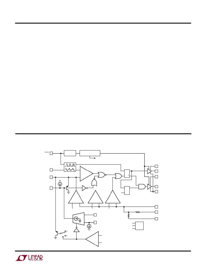
�BLOCK� DIAGRA�
�V� CC� (Pin� 14/Pin� 7/Pin� 7):� Power� Supply� Input.� All� low�
�power� internal� circuits� draw� their� supply� from� this� pin.�
�Connect� this� pin� to� a� clean� power� supply,� separate� from�
�the� main� V� IN� supply� at� the� drain� of� Q1.� This� pin� requires� a�
�4.7� μ� F� bypass� capacitor.� The� LTC3830-1� and� the� 8-lead�
�LTC3830� have� V� CC� and� PV� CC2� tied� together� at� Pin� 7� and�
�require a 10μF bypass capacitor to GND.�
�PV� CC2� (Pin� 15/Pin� 7/Pin� 7):� Power� Supply� Input� for� G2.�
�Connect� this� pin� to� the� main� high� power� supply.�
�G2� (Pin� 16/Pin� 8/Pin� 8):� Bottom� Gate� Driver� Output.�
�Connect� this� pin� to� the� gate� of� the� lower� N-channel�
�MOSFET,� Q2.� This� output� swings� from� PGND� to� PV� CC2� .� It�
�remains� low� when� G1� is� high� or� during� shutdown� mode.�
�To� prevent� output� undershoot� during� a� soft-start� cycle,� G2�
�is� held� low� until� G1� first� goes� high.� (FFBG� in� Block�
�Diagram.)�
�SHDN�
�100ms� DELAY�
�INTERNAL�
�LOGIC� AND�
�THERMAL� SHUTDOWN�
�POWER� DOWN�
�DISDR�
�OSCILLATOR�
�PV� CC1�
�FREQSET�
�S�
�Q�
�G1�
�PWM�
�COMP�
�R�
�Q�
�PV� CC2�
�SS�
�12� μ� A�
�QSS�
�POR�
�FFBG�
�S� Q�
�R�
�ENABLE�
�G2�
�G2�
�PGND�
�ERR�
�MIN�
�MAX�
�+�
�–�
�–�
�+�
�–�
�+�
�FB�
�V� REF�
�CC�
�–�
�V� REF� –� 3%�
�I� FB�
�V� REF� +� 3%�
�11.2k�
�18k�
�SENSE� +�
�SENSE� –�
�+�
�I� MAX�
�V� REF�
�2.2V�
�12� μ� A�
�V� REF� –� 3%�
�V� REF� +� 3%�
�BG�
�3830� BD�
�QC�
�1.2V�
�DISABLE�
�ILIM�
�+�
�PV� CC1�
�V�
�–�
�V� CC1� +� 2.5V�
�3830fa�
�7�
�相关PDF资料 |
PDF描述 |
|---|---|
| SPD62-153M | INDUCTOR PWR SHIELDED 15.0UH SMD |
| LTC3830ES | IC REG CTRLR BUCK PWM VM 16-SOIC |
| LTC1771IS8#PBF | IC REG CTRLR BUCK PWM CM 8-SOIC |
| LTC1735CGN-1#PBF | IC REG CTRLR BUCK PWM CM 16-SSOP |
| SPD62-123M | INDUCTOR PWR SHIELDED 12.0UH SMD |
相关代理商/技术参数 |
参数描述 |
|---|---|
| LTC3831EGN | 功能描述:IC SW REG CONTROLLR SYNC 16-SSOP RoHS:否 类别:集成电路 (IC) >> PMIC - 稳压器 - 专用型 系列:- 标准包装:43 系列:- 应用:控制器,Intel VR11 输入电压:5 V ~ 12 V 输出数:1 输出电压:0.5 V ~ 1.6 V 工作温度:-40°C ~ 85°C 安装类型:表面贴装 封装/外壳:48-VFQFN 裸露焊盘 供应商设备封装:48-QFN(7x7) 包装:管件 |
| LTC3831EGN#PBF | 功能描述:IC SW REG CONTROLLR SYNC 16-SSOP RoHS:是 类别:集成电路 (IC) >> PMIC - 稳压器 - 专用型 系列:- 标准包装:43 系列:- 应用:控制器,Intel VR11 输入电压:5 V ~ 12 V 输出数:1 输出电压:0.5 V ~ 1.6 V 工作温度:-40°C ~ 85°C 安装类型:表面贴装 封装/外壳:48-VFQFN 裸露焊盘 供应商设备封装:48-QFN(7x7) 包装:管件 |
| LTC3831EGN#TR | 功能描述:IC SW REG CONTROLLR SYNC 16-SSOP RoHS:否 类别:集成电路 (IC) >> PMIC - 稳压器 - 专用型 系列:- 标准包装:43 系列:- 应用:控制器,Intel VR11 输入电压:5 V ~ 12 V 输出数:1 输出电压:0.5 V ~ 1.6 V 工作温度:-40°C ~ 85°C 安装类型:表面贴装 封装/外壳:48-VFQFN 裸露焊盘 供应商设备封装:48-QFN(7x7) 包装:管件 |
| LTC3831EGN#TRPBF | 功能描述:IC SW REG CONTROLLR SYNC 16-SSOP RoHS:是 类别:集成电路 (IC) >> PMIC - 稳压器 - 专用型 系列:- 标准包装:43 系列:- 应用:控制器,Intel VR11 输入电压:5 V ~ 12 V 输出数:1 输出电压:0.5 V ~ 1.6 V 工作温度:-40°C ~ 85°C 安装类型:表面贴装 封装/外壳:48-VFQFN 裸露焊盘 供应商设备封装:48-QFN(7x7) 包装:管件 |
| LTC3831EGN-1 | 功能描述:IC CTRLR SW REG SYNC DDR 16SSOP RoHS:否 类别:集成电路 (IC) >> PMIC - 稳压器 - 专用型 系列:- 标准包装:43 系列:- 应用:控制器,Intel VR11 输入电压:5 V ~ 12 V 输出数:1 输出电压:0.5 V ~ 1.6 V 工作温度:-40°C ~ 85°C 安装类型:表面贴装 封装/外壳:48-VFQFN 裸露焊盘 供应商设备封装:48-QFN(7x7) 包装:管件 |
发布紧急采购,3分钟左右您将得到回复。