- 您现在的位置:买卖IC网 > PDF目录80071 > LTC3851AHMSE-1#PBF (LINEAR TECHNOLOGY CORP) 0.05 A SWITCHING CONTROLLER, 810 kHz SWITCHING FREQ-MAX, PDSO16 PDF资料下载
参数资料
| 型号: | LTC3851AHMSE-1#PBF |
| 厂商: | LINEAR TECHNOLOGY CORP |
| 元件分类: | 稳压器 |
| 英文描述: | 0.05 A SWITCHING CONTROLLER, 810 kHz SWITCHING FREQ-MAX, PDSO16 |
| 封装: | LEAD FREE, PLASTIC, MSOP-16 |
| 文件页数: | 17/30页 |
| 文件大小: | 0K |
| 代理商: | LTC3851AHMSE-1#PBF |
第1页第2页第3页第4页第5页第6页第7页第8页第9页第10页第11页第12页第13页第14页第15页第16页当前第17页第18页第19页第20页第21页第22页第23页第24页第25页第26页第27页第28页第29页第30页
LTC3851A-1
24
3851a1fa
applicaTions inForMaTion
2. Does the VFB pin connect directly to the feedback resis-
tors? The resistive divider R1, R2 must be connected
between the (+) plate of COUT and signal ground. The
47pF to 100pF capacitor should be as close as possible
to the LTC3851A-1. Be careful locating the feedback
resistors too far away from the LTC3851A-1. The VFB
line should not be routed close to any other nodes with
high slew rates.
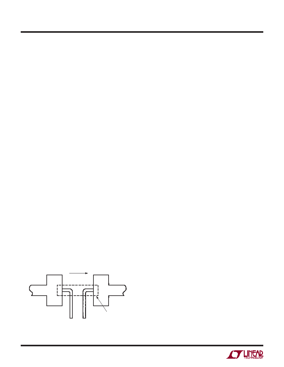
3. Are the SENSE– and SENSE+ leads routed together
with minimum PC trace spacing? The filter capacitor
between SENSE+ and SENSE– should be as close as
possible to the LTC3851A-1. Ensure accurate current
sensing with Kelvin connections as shown in Figure 10.
Series resistance can be added to the SENSE lines to
increase noise rejection and to compensate for the ESL
of RSENSE.
4. Does the (+) terminal of CIN connect to the drain of
the topside MOSFET(s) as closely as possible? This
capacitor provides the AC current to the MOSFET(s).
5. Is the INTVCC decoupling capacitor connected closely
between INTVCC and GND? This capacitor carries the
MOSFETdriverpeakcurrents.Anadditional1μFceramic
capacitor placed immediately next to the INTVCC and
GND pins can help improve noise performance.
6. Keep the switching node (SW), top gate node (TG) and
boost node (BOOST) away from sensitive small-signal
nodes, especially from the voltage and current sensing
feedback pins. All of these nodes have very large and
fast moving signals and therefore should be kept on
the “output side” (Pin 9 to Pin 16) of the LTC3851A-1
and occupy minimum PC trace area.
PC Board Layout Debugging
It is helpful to use a DC-50MHz current probe to monitor
thecurrentintheinductorwhiletestingthecircuit.Monitor
the output switching node (SW pin) to synchronize the
oscilloscope to the internal oscillator and probe the actual
output voltage as well. Check for proper performance over
the operating voltage and current range expected in the
application. The frequency of operation should be main-
tained over the input voltage range down to dropout and
until the output load drops below the low current opera-
tion threshold—typically 10% of the maximum designed
current level in Burst Mode operation.
Thedutycyclepercentageshouldbemaintainedfromcycle
to cycle in a well designed, low noise PCB implementation.
Variation in the duty cycle at a subharmonic rate can sug-
gest noise pick-up at the current or voltage sensing inputs
or inadequate loop compensation. Overcompensation of
the loop can be used to tame a poor PC layout if regulator
bandwidth optimization is not required.
Reduce VIN from its nominal level to verify operation
of the regulator in dropout. Check the operation of the
undervoltage lockout circuit by further lowering VIN while
monitoring the outputs to verify operation.
Investigate whether any problems exist only at higher out-
put currents or only at higher input voltages. If problems
coincide with high input voltages and low output currents,
look for capacitive coupling between the BOOST, SW, TG
and possibly BG connections and the sensitive voltage
and current pins. The capacitor placed across the current
sensing pins needs to be placed immediately adjacent to
the pins of the IC. This capacitor helps to minimize the
effects of differential noise injection due to high frequency
capacitive coupling. If problems are encountered with
high current output loading at lower input voltages, look
for inductive coupling between CIN, the Schottky and the
top MOSFET to the sensitive current and voltage sens-
ing traces. In addition, investigate common ground path
voltage pickup between these components and the GND
pin of the IC.
Figure 10. Kelvin Sensing RSENSE
SENSE+ SENSE–
HIGH CURRENT PATH
3851A1 F10
CURRENT SENSE
RESISTOR
(RSENSE)
相关PDF资料 |
PDF描述 |
|---|---|
| LPD48SP | 1-OUTPUT 75 W DC-DC REG PWR SUPPLY MODULE |
| LM2575S-12 | 3.2 A SWITCHING REGULATOR, 62 kHz SWITCHING FREQ-MAX, PSSO5 |
| LK1601-7ERD0TB1 | 1-OUTPUT 150 W AC-DC REG PWR SUPPLY MODULE |
| LT1074HVCV | 5.5 A SWITCHING REGULATOR, 200 kHz SWITCHING FREQ-MAX, PSIP11 |
| LES010YE | 1-OUTPUT 15 W DC-DC REG PWR SUPPLY MODULE |
相关代理商/技术参数 |
参数描述 |
|---|---|
| LTC3851AIGN#PBF | 功能描述:IC REG CTRLR BUCK PWM CM 16-SSOP RoHS:是 类别:集成电路 (IC) >> PMIC - 稳压器 - DC DC 切换控制器 系列:- 标准包装:2,500 系列:- PWM 型:电流模式 输出数:1 频率 - 最大:500kHz 占空比:96% 电源电压:4 V ~ 36 V 降压:无 升压:是 回扫:无 反相:无 倍增器:无 除法器:无 Cuk:无 隔离:无 工作温度:-40°C ~ 125°C 封装/外壳:24-WQFN 裸露焊盘 包装:带卷 (TR) |
| LTC3851AIGN#TRPBF | 功能描述:IC REG CTRLR BUCK PWM CM 16-SSOP RoHS:是 类别:集成电路 (IC) >> PMIC - 稳压器 - DC DC 切换控制器 系列:- 标准包装:2,500 系列:- PWM 型:电流模式 输出数:1 频率 - 最大:500kHz 占空比:96% 电源电压:4 V ~ 36 V 降压:无 升压:是 回扫:无 反相:无 倍增器:无 除法器:无 Cuk:无 隔离:无 工作温度:-40°C ~ 125°C 封装/外壳:24-WQFN 裸露焊盘 包装:带卷 (TR) |
| LTC3851AIMSE#PBF | 功能描述:IC REG CTRLR BUCK PWM CM 16-MSOP RoHS:是 类别:集成电路 (IC) >> PMIC - 稳压器 - DC DC 切换控制器 系列:- 标准包装:2,500 系列:- PWM 型:电流模式 输出数:1 频率 - 最大:500kHz 占空比:96% 电源电压:4 V ~ 36 V 降压:无 升压:是 回扫:无 反相:无 倍增器:无 除法器:无 Cuk:无 隔离:无 工作温度:-40°C ~ 125°C 封装/外壳:24-WQFN 裸露焊盘 包装:带卷 (TR) |
| LTC3851AIMSE#TRPBF | 功能描述:IC REG CTRLR BUCK PWM CM 16-MSOP RoHS:是 类别:集成电路 (IC) >> PMIC - 稳压器 - DC DC 切换控制器 系列:- 标准包装:2,500 系列:- PWM 型:电流模式 输出数:1 频率 - 最大:500kHz 占空比:96% 电源电压:4 V ~ 36 V 降压:无 升压:是 回扫:无 反相:无 倍增器:无 除法器:无 Cuk:无 隔离:无 工作温度:-40°C ~ 125°C 封装/外壳:24-WQFN 裸露焊盘 包装:带卷 (TR) |
| LTC3851AIMSE-1#PBF | 功能描述:IC REG CTRLR BUCK PWM CM 16-MSOP RoHS:是 类别:集成电路 (IC) >> PMIC - 稳压器 - DC DC 切换控制器 系列:- 标准包装:2,500 系列:- PWM 型:电流模式 输出数:1 频率 - 最大:500kHz 占空比:96% 电源电压:4 V ~ 36 V 降压:无 升压:是 回扫:无 反相:无 倍增器:无 除法器:无 Cuk:无 隔离:无 工作温度:-40°C ~ 125°C 封装/外壳:24-WQFN 裸露焊盘 包装:带卷 (TR) |
发布紧急采购,3分钟左右您将得到回复。