- 您现在的位置:买卖IC网 > PDF目录15302 > LTC3866EFE#TRPBF (Linear Technology)IC REG CTRLR BUCK PWM CM 24TSSOP PDF资料下载
参数资料
| 型号: | LTC3866EFE#TRPBF |
| 厂商: | Linear Technology |
| 文件页数: | 13/36页 |
| 文件大小: | 0K |
| 描述: | IC REG CTRLR BUCK PWM CM 24TSSOP |
| 标准包装: | 2,500 |
| PWM 型: | 电流模式 |
| 输出数: | 1 |
| 频率 - 最大: | 850kHz |
| 占空比: | 95% |
| 电源电压: | 4.5 V ~ 38 V |
| 降压: | 是 |
| 升压: | 无 |
| 回扫: | 无 |
| 反相: | 无 |
| 倍增器: | 无 |
| 除法器: | 无 |
| Cuk: | 无 |
| 隔离: | 无 |
| 工作温度: | -40°C ~ 125°C |
| 封装/外壳: | 24-TSSOP(0.173",4.40mm)裸露焊盘 |
| 包装: | 带卷 (TR) |
第1页第2页第3页第4页第5页第6页第7页第8页第9页第10页第11页第12页当前第13页第14页第15页第16页第17页第18页第19页第20页第21页第22页第23页第24页第25页第26页第27页第28页第29页第30页第31页第32页第33页第34页第35页第36页
�� �
�
�LTC3866�
�OPERATION�
�+�
�C� OUT�
�–�
�IftheMODE/PLLINpinisnotbeingdrivenbyanexternal�
�clock� source,� the� FREQ� pin� can� be� used� to� program� the�
�controller’s� operating� frequency� from� 250kHz� to� 770kHz.�
�There� is� a� precision� 10μA� current� flowing� out� of� the� FREQ�
�pin� so� that� the� user� can� program� the� controller’s� switch-�
�ing� frequency� with� a� single� resistor� to� SGND.� A� curve�
�is� provided� later� in� the� Applications� Information� section�
�showing� the� relationship� between� the� voltage� on� the� FREQ�
�pin� and� switching� frequency.�
�A� phase-locked� loop� (PLL)� is� available� on� the� LTC3866�
�to� synchronize� the� internal� oscillator� to� an� external� clock�
�source� that� is� connected� to� the� MODE/PLLIN� pin.� The� PLL�
�loop� filter� network� is� integrated� inside� the� LTC3866.� The�
�phase-locked� loop� is� capable� of� locking� any� frequency�
�within� the� range� of� 250kHz� to� 770kHz.� The� frequency� setting�
�resistor� should� always� be� present� to� set� the� controller’s�
�initial� switching� frequency� before� locking� to� the� external�
�clock.� The� controller� operates� in� forced� continuous� mode�
�when� it� is� synchronized.�
�Sensing� the� Output� Voltage� with� a�
�Differential� Amplifier�
�The� LTC3866� includes� a� low� offset,� high� input� impedance,�
�unity-gain,� high� bandwidth� differential� amplifier� for� ap-�
�plications� that� require� true� remote� sensing.� Sensing� the�
�load� across� the� load� capacitors� directly� greatly� benefits�
�regulation� in� high� current,� low� voltage� applications,� where�
�board� interconnection� losses� can� be� a� significant� portion�
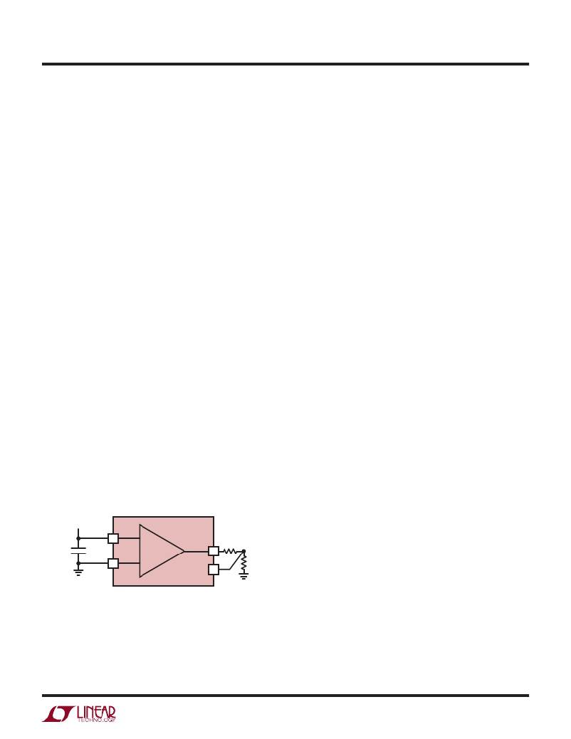
�of� the� total� error� budget.� Connect� DIFFP� to� the� output� load,�
�and� DIFFN� to� the� load� ground.� See� Figure� 1.�
�V� OUT� LTC3866�
�DIFFP�
�8�
�DIFFOUT�
�DIFFAMP� 6�
�DIFFN�
�7�
�V� FB� 5�
�3866� F01�
�Figure� 1.� Differential� Amplifier� Connection�
�The� LTC3866� differential� amplifier� has� a� typical� output� slew�
�rate� of� 2V/μs.� The� amplifier� is� configured� for� unity� gain,�
�meaning� that� the� difference� between� DIFFP� and� DIFFN� is�
�translated� to� DIFFOUT,� relative� to� SGND.�
�Care� should� be� taken� to� route� the� DIFFP� and� DIFFN� PCB�
�traces� parallel� to� each� other� all� the� way� to� the� remote� sens-�
�ing� points� on� the� board.� In� addition,� avoid� routing� these�
�sensitive� traces� near� any� high� speed� switching� nodes� in�
�the� circuit.� Ideally,� the� DIFFP� and� DIFFN� traces� should� be�
�shielded� by� a� low� impedance� ground� plane� to� maintain�
�signal� integrity.�
�Power� Good� (PGOOD� Pin)�
�The� PGOOD� pin� is� connected� to� the� open� drain� of� an�
�internal� N-channel� MOSFET.� The� MOSFET� turns� on� and�
�pulls� the� PGOOD� pin� low� when� the� V� FB� pin� voltage� is� not�
�within� ±10%� of� the� 0.6V� reference� voltage.� The� PGOOD�
�pin� is� also� pulled� low� when� the� RUN� pin� is� below� 1.14V� or�
�when� the� LTC3866� is� in� the� soft-start� or� tracking� up� phase.�
�When� the� V� FB� pin� voltage� is� within� the� ±10%� regulation�
�window,� the� MOSFET� is� turned� off� and� the� pin� is� allowed�
�to� be� pulled� up� by� an� external� resistor� to� a� source� of� up�
�to� 6V.� The� PGOOD� pin� will� flag� power� good� immediately�
�when� the� V� FB� pin� is� within� the� regulation� window.� However,�
�there� is� an� internal� 20μs� power-bad� mask� when� the� V� FB�
�goes� out� of� the� window.�
�Output� Overvoltage� Protection�
�An� overvoltage� comparator,� OV,� guards� against� transient�
�overshoots� (>10%)� as� well� as� other� more� serious� condi-�
�tions� that� may� overvoltage� the� output.� In� such� cases,� the�
�top� MOSFET� is� turned� off� and� the� bottom� MOSFET� is� turned�
�on� until� the� overvoltage� condition� is� cleared.�
�Undervoltage� Lockout�
�The� LTC3866� has� two� functions� that� help� protect� the�
�controller� in� case� of� undervoltage� conditions.� A� precision�
�UVLO� comparator� constantly� monitors� the� INTV� CC� voltage�
�to� ensure� that� an� adequate� gate-drive� voltage� is� present.�
�It� locks� out� the� switching� action� when� INTV� CC� is� below�
�3.75V.� To� prevent� oscillation� when� there� is� a� disturbance�
�on� the� INTV� CC� ,� the� UVLO� comparator� has� 600mV� of� preci-�
�sion� hysteresis.�
�3866fb�
�13�
�相关PDF资料 |
PDF描述 |
|---|---|
| EEM43DREF | CONN EDGECARD 86POS .156 EYELET |
| VI-JWL-EW-F4 | CONVERTER MOD DC/DC 28V 100W |
| LTC3865IFE#TRPBF | IC REG CTRLR BUCK PWM CM 38TSSOP |
| VI-JWL-EW-F2 | CONVERTER MOD DC/DC 28V 100W |
| EBA49DRMN | CONN EDGECARD 98POS .125 SQ WW |
相关代理商/技术参数 |
参数描述 |
|---|---|
| LTC3866EUF#PBF | 功能描述:IC REG CTRLR BUCK PWM CM 24-QFN RoHS:是 类别:集成电路 (IC) >> PMIC - 稳压器 - DC DC 切换控制器 系列:- 标准包装:2,500 系列:- PWM 型:电流模式 输出数:1 频率 - 最大:500kHz 占空比:96% 电源电压:4 V ~ 36 V 降压:无 升压:是 回扫:无 反相:无 倍增器:无 除法器:无 Cuk:无 隔离:无 工作温度:-40°C ~ 125°C 封装/外壳:24-WQFN 裸露焊盘 包装:带卷 (TR) |
| LTC3866EUF#TRPBF | 功能描述:IC REG CTRLR BUCK PWM CM 24-QFN RoHS:是 类别:集成电路 (IC) >> PMIC - 稳压器 - DC DC 切换控制器 系列:- 标准包装:2,500 系列:- PWM 型:电流模式 输出数:1 频率 - 最大:500kHz 占空比:96% 电源电压:4 V ~ 36 V 降压:无 升压:是 回扫:无 反相:无 倍增器:无 除法器:无 Cuk:无 隔离:无 工作温度:-40°C ~ 125°C 封装/外壳:24-WQFN 裸露焊盘 包装:带卷 (TR) |
| LTC3866IFE#PBF | 功能描述:IC REG CTRLR BUCK PWM CM 24TSSOP RoHS:是 类别:集成电路 (IC) >> PMIC - 稳压器 - DC DC 切换控制器 系列:- 标准包装:2,000 系列:- PWM 型:电流模式 输出数:1 频率 - 最大:1MHz 占空比:50% 电源电压:9 V ~ 10 V 降压:无 升压:是 回扫:是 反相:无 倍增器:无 除法器:无 Cuk:无 隔离:无 工作温度:-40°C ~ 85°C 封装/外壳:8-TSSOP(0.173",4.40mm 宽) 包装:带卷 (TR) |
| LTC3866IFE#PBF | 制造商:Linear Technology 功能描述:BUCK REGULATOR CURRENT MODE SYNC TSSOP |
| LTC3866IFE#TRPBF | 功能描述:IC REG CTRLR BUCK PWM CM 24TSSOP RoHS:是 类别:集成电路 (IC) >> PMIC - 稳压器 - DC DC 切换控制器 系列:- 标准包装:2,500 系列:- PWM 型:电流模式 输出数:1 频率 - 最大:500kHz 占空比:96% 电源电压:4 V ~ 36 V 降压:无 升压:是 回扫:无 反相:无 倍增器:无 除法器:无 Cuk:无 隔离:无 工作温度:-40°C ~ 125°C 封装/外壳:24-WQFN 裸露焊盘 包装:带卷 (TR) |
发布紧急采购,3分钟左右您将得到回复。