- 您现在的位置:买卖IC网 > PDF目录15302 > LTC3866EFE#TRPBF (Linear Technology)IC REG CTRLR BUCK PWM CM 24TSSOP PDF资料下载
参数资料
| 型号: | LTC3866EFE#TRPBF |
| 厂商: | Linear Technology |
| 文件页数: | 19/36页 |
| 文件大小: | 0K |
| 描述: | IC REG CTRLR BUCK PWM CM 24TSSOP |
| 标准包装: | 2,500 |
| PWM 型: | 电流模式 |
| 输出数: | 1 |
| 频率 - 最大: | 850kHz |
| 占空比: | 95% |
| 电源电压: | 4.5 V ~ 38 V |
| 降压: | 是 |
| 升压: | 无 |
| 回扫: | 无 |
| 反相: | 无 |
| 倍增器: | 无 |
| 除法器: | 无 |
| Cuk: | 无 |
| 隔离: | 无 |
| 工作温度: | -40°C ~ 125°C |
| 封装/外壳: | 24-TSSOP(0.173",4.40mm)裸露焊盘 |
| 包装: | 带卷 (TR) |
第1页第2页第3页第4页第5页第6页第7页第8页第9页第10页第11页第12页第13页第14页第15页第16页第17页第18页当前第19页第20页第21页第22页第23页第24页第25页第26页第27页第28页第29页第30页第31页第32页第33页第34页第35页第36页
�� �
�
�LTC3866�
�APPLICATIONS� INFORMATION�
�V�
�V� GS�
�MILLER� EFFECT�
�a� b�
�+�
�Q� IN� V� GS�
�C� MILLER� =� (Q� B� –� Q� A� )/V� DS� –�
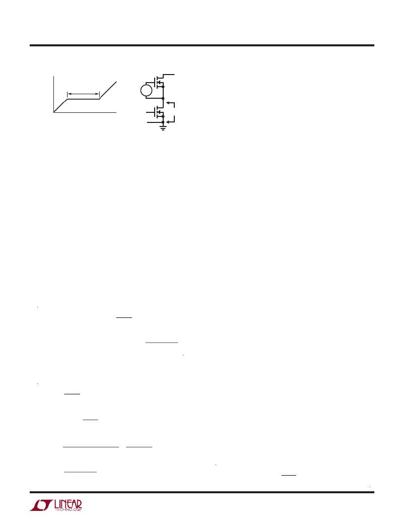
�Figure� 7.� Gate� Charge� Characteristic�
�V� IN�
�+� V� DS�
�–�
�3766� F07�
�where� δ� is� the� temperature� dependency� of� R� DS(ON)� ,� R� DR�
�is� the� effective� top� driver� resistance� (approximately� 2Ω� at�
�V� GS� =� V� MILLER� ),� V� IN� is� the� drain� potential� and� the� change�
�in� drain� potential� in� the� particular� application.� V� TH(MIN)�
�is� the� data� sheet� specified� typical� gate� threshold� voltage�
�specified� in� the� power� MOSFET� data� sheet� at� the� specified�
�drain� current.� C� MILLER� is� the� calculated� capacitance� using�
�the� gate� charge� curve� from� the� MOSFET� data� sheet� and�
�the� technique� described� above.�
�V� OUT�
�?� V� –� V� OUT� ?�
�Synchronous� Switch� Duty� Cycle� =� ?� IN� ?�
�(�
�)�
�V� OUT�
�(� )� R� DS(ON)� +�
�P� MAIN� =�
�1� +� δ�
�I� MAX�
�?� (� R� DR� )� (� C� MILLER� )� ?�
�(� V� IN� )� ?�
�?� ?�
�?�
�?� ?� f�
�+�
�(�
�)�
�V� IN� –� V� OUT�
�(� 1� +� δ� )� R� DS(ON)�
�P� SYNC� =�
�I� MAX�
�I� MAX� ?�
�?� (� V� OUT� )� (� V� IN� –� V� OUT� )� ??�
�C� IN� Required� I� RMS� ≈�
�due to the drain-to-gate accumulation capacitance and�
�the� gate-to-source� capacitance.� The� Miller� charge� (the�
�increase� in� coulombs� on� the� horizontal� axis� from� a� to� b�
�while� the� curve� is� flat)� is� specified� for� a� given� V� DS� drain�
�voltage,� but� can� be� adjusted� for� different� V� DS� voltages� by�
�multiplying� the� ratio� of� the� application� V� DS� to� the� curve�
�specified� V� DS� values.� A� way� to� estimate� the� C� MILLER� term�
�is� to� take� the� change� in� gate� charge� from� points� a� and� b�
�on� a� manufacturer’s� data� sheet� and� divide� by� the� stated�
�V� DS� voltage� specified.� C� MILLER� is� the� most� important� se-�
�lection� criteria� for� determining� the� transition� loss� term� in�
�the� top� MOSFET� but� is� not� directly� specified� on� MOSFET�
�data� sheets.� C� RSS� and� C� OS� are� specified� sometimes� but�
�definitions� of� these� parameters� are� not� included.� When� the�
�controller� is� operating� in� continuous� mode� the� duty� cycles�
�for� the� top� and� bottom� MOSFETs� are� given� by:�
�Main� Switch� Duty� Cycle� =�
�V� IN�
�?� V� IN� ?�
�The� power� dissipation� for� the� main� and� synchronous�
�MOSFETs� at� maximum� output� current� are� given� by:�
�2�
�V� IN�
�2� ?� I� MAX� ?�
�?� 2� ?�
�1� 1�
�?� ?�
�?� V� INTVCC� –� V� TH(MIN)� V� TH(MIN)� ?�
�2�
�V� IN�
�Both� MOSFETs� have� I� 2� R� losses� while� the� topside� N-channel�
�equation� includes� an� additional� term� for� transition� losses,�
�which� peak� at� the� highest� input� voltage.� For� V� IN� <� 20V,�
�the� high� current� efficiency� generally� improves� with� larger�
�MOSFETs,� while� for� V� IN� >� 20V,� the� transition� losses� rapidly�
�increase� to� the� point� that� the� use� of� a� higher� R� DS(ON)� device�
�with� lower� C� MILLER� actually� provides� higher� efficiency.� The�
�synchronous� MOSFET� losses� are� greatest� at� high� input�
�voltage� when� the� top� switch� duty� factor� is� low� or� during�
�a� short-circuit� when� the� synchronous� switch� is� on� close�
�to� 100%� of� the� period.�
�The� term� (1� +� δ� )� is� generally� given� for� a� MOSFET� in� the�
�form� of� a� normalized� R� DS(ON)� vs� temperature� curve,� but�
�δ� =� 0.005/°C� can� be� used� as� an� approximation� for� low�
�voltage� MOSFETs.�
�An� optional� Schottky� diode� across� the� synchronous�
�MOSFET� conducts� during� the� dead� time� between� the� con-�
�duction� of� the� two� large� power� MOSFETs.� This� prevents� the�
�body� diode� of� the� bottom� MOSFET� from� turning� on,� storing�
�charge� during� the� dead� time� and� requiring� a� reverse-recov-�
�ery� period� which� could� cost� as� much� as� several� percent� in�
�efficiency.� A� 2A� to� 8A� Schottky� is� generally� a� good� com-�
�promise� for� both� regions� of� operation� due� to� the� relatively�
�small� average� current.� Larger� diodes� result� in� additional�
�transition� loss� due� to� their� larger� junction� capacitance.�
�C� IN� and� C� OUT� Selection�
�In� continuous� mode,� the� source� current� of� the� top� MOSFET�
�is� a� square� wave� of� duty� cycle� (V� OUT� )/(V� IN� ).� To� prevent�
�large� voltage� transients,� a� low� ESR� capacitor� sized� for� the�
�maximum� RMS� current� of� one� channel� must� be� used.� The�
�maximum� RMS� capacitor� current� is� given� by:�
�1/2�
�V� IN�
�3866fb�
�19�
�相关PDF资料 |
PDF描述 |
|---|---|
| EEM43DREF | CONN EDGECARD 86POS .156 EYELET |
| VI-JWL-EW-F4 | CONVERTER MOD DC/DC 28V 100W |
| LTC3865IFE#TRPBF | IC REG CTRLR BUCK PWM CM 38TSSOP |
| VI-JWL-EW-F2 | CONVERTER MOD DC/DC 28V 100W |
| EBA49DRMN | CONN EDGECARD 98POS .125 SQ WW |
相关代理商/技术参数 |
参数描述 |
|---|---|
| LTC3866EUF#PBF | 功能描述:IC REG CTRLR BUCK PWM CM 24-QFN RoHS:是 类别:集成电路 (IC) >> PMIC - 稳压器 - DC DC 切换控制器 系列:- 标准包装:2,500 系列:- PWM 型:电流模式 输出数:1 频率 - 最大:500kHz 占空比:96% 电源电压:4 V ~ 36 V 降压:无 升压:是 回扫:无 反相:无 倍增器:无 除法器:无 Cuk:无 隔离:无 工作温度:-40°C ~ 125°C 封装/外壳:24-WQFN 裸露焊盘 包装:带卷 (TR) |
| LTC3866EUF#TRPBF | 功能描述:IC REG CTRLR BUCK PWM CM 24-QFN RoHS:是 类别:集成电路 (IC) >> PMIC - 稳压器 - DC DC 切换控制器 系列:- 标准包装:2,500 系列:- PWM 型:电流模式 输出数:1 频率 - 最大:500kHz 占空比:96% 电源电压:4 V ~ 36 V 降压:无 升压:是 回扫:无 反相:无 倍增器:无 除法器:无 Cuk:无 隔离:无 工作温度:-40°C ~ 125°C 封装/外壳:24-WQFN 裸露焊盘 包装:带卷 (TR) |
| LTC3866IFE#PBF | 功能描述:IC REG CTRLR BUCK PWM CM 24TSSOP RoHS:是 类别:集成电路 (IC) >> PMIC - 稳压器 - DC DC 切换控制器 系列:- 标准包装:2,000 系列:- PWM 型:电流模式 输出数:1 频率 - 最大:1MHz 占空比:50% 电源电压:9 V ~ 10 V 降压:无 升压:是 回扫:是 反相:无 倍增器:无 除法器:无 Cuk:无 隔离:无 工作温度:-40°C ~ 85°C 封装/外壳:8-TSSOP(0.173",4.40mm 宽) 包装:带卷 (TR) |
| LTC3866IFE#PBF | 制造商:Linear Technology 功能描述:BUCK REGULATOR CURRENT MODE SYNC TSSOP |
| LTC3866IFE#TRPBF | 功能描述:IC REG CTRLR BUCK PWM CM 24TSSOP RoHS:是 类别:集成电路 (IC) >> PMIC - 稳压器 - DC DC 切换控制器 系列:- 标准包装:2,500 系列:- PWM 型:电流模式 输出数:1 频率 - 最大:500kHz 占空比:96% 电源电压:4 V ~ 36 V 降压:无 升压:是 回扫:无 反相:无 倍增器:无 除法器:无 Cuk:无 隔离:无 工作温度:-40°C ~ 125°C 封装/外壳:24-WQFN 裸露焊盘 包装:带卷 (TR) |
发布紧急采购,3分钟左右您将得到回复。