- 您现在的位置:买卖IC网 > PDF目录30772 > LTC4219IDHC-12#TRPBF (LINEAR TECHNOLOGY CORP) 1-CHANNEL POWER SUPPLY SUPPORT CKT, PDSO16 PDF资料下载
参数资料
| 型号: | LTC4219IDHC-12#TRPBF |
| 厂商: | LINEAR TECHNOLOGY CORP |
| 元件分类: | 电源管理 |
| 英文描述: | 1-CHANNEL POWER SUPPLY SUPPORT CKT, PDSO16 |
| 封装: | 5 X 3 MM, LEAD FREE, PLASTIC, MO-229WJED-1, DFN-16 |
| 文件页数: | 4/18页 |
| 文件大小: | 195K |
| 代理商: | LTC4219IDHC-12#TRPBF |
LTC4219
12
4219fb
APPLICATIONS INFORMATION
Turn-Off Sequence
The switch can be turned off by a variety of conditions. A
normal turn-off is initiated by either the EN1 or EN2 pins
going above their 1.235V threshold. Additionally, several
fault conditions will turn off the switch. These include
overcurrent circuit breaker (SENSE pin) or overtem-
perature. Normally the switch is turned off with a 250μA
current pulling down the GATE pin to ground. With the
switch turned off, the OUT voltage drops which pulls the
FB pin below its threshold. PG then goes high to indicate
output power is no longer good.
If VDD drops below 2.65V for greater than 5μs or INTVCC
drops below 2.5V for greater than 1μs, a fast shutdown
of the switch is initiated. The GATE is pulled down with a
140mA current to the OUT pin.
Overcurrent Fault
The LTC4219 features an adjustable current limit with
foldback that protects against short circuits or excessive
load current. To prevent excessive power dissipation in the
switch during active current limit, the available current is
reduced as a function of the output voltage sensed by the
FB pin. A graph in the Typical Performance Characteristics
curves shows the current limit versus FB voltage.
An overcurrent fault occurs when the current limit circuitry
has been engaged for longer than the time-out delay set
by the TIMER. Current limiting begins when the MOSFET
current reaches 1.5A to 5.6A (depending on the foldback).
The GATE pin is then brought down with a 140mA GATE-
to-OUT current. The voltage on the GATE is regulated in
order to limit the current to less than 5.6A. At this point,
a circuit breaker time delay starts by charging the external
timing capacitor from the TIMER pin with a 100μA pull-
up current. If the TIMER pin reaches its 1.2V threshold,
the internal switch turns off (with a 250μA current from
GATE to ground). Included in the Typical Performance
Characteristics curves is a graph of the Safe Operating
Area for the MOSFET. From this graph one can determine
the MOSFET’s maximum time in current limit for a given
output power.
Adding a capacitor and a 1k series resistor from GATE
to ground will lower the inrush current below the default
value set by the inrush circuit. The GATE is then charged
with a 24μA current source. The voltage at the GATE pin
rises with a slope equal to 24μA/CGATE and the supply
inrush current is set at:
I
INRUSH =
C
L
C
GATE
24A
When the GATE voltage reaches the MOSFET threshold
voltage, the switch begins to turn on and the OUT voltage
follows the GATE voltage as it increases. Once OUT reaches
VDD, the GATE will ramp up until clamped by the 6.15V
Zener between GATE and OUT.
As the OUT voltage rises, so will the FB pin which is moni-
toring it. Once the FB pin crosses its 1.235V threshold and
the GATE to OUT voltage exceeds 4.2V, the PG pin pulls
low indicating that the power is good.
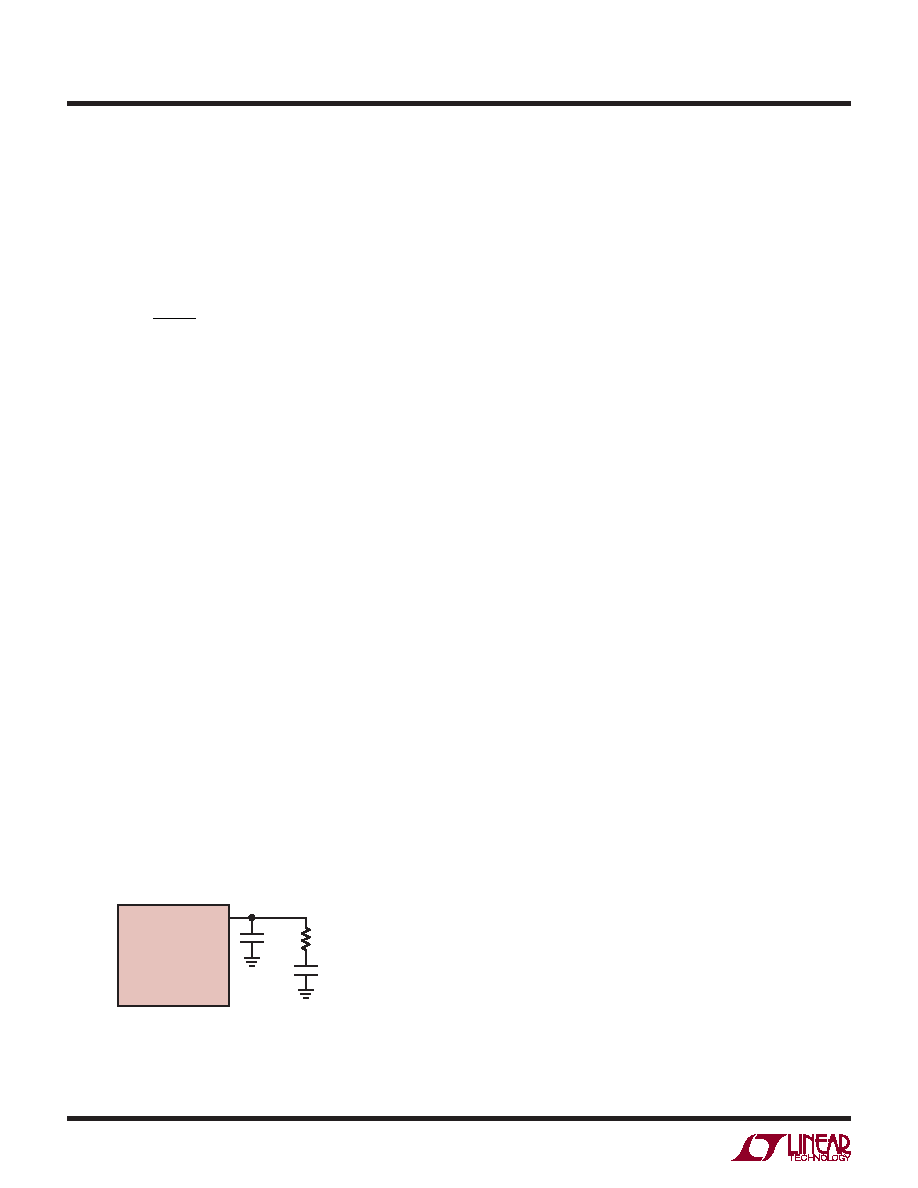
Parasitic MOSFET Oscillation
When the N-channel MOSFET ramps up the output dur-
ing power-up it operates as a source follower. The source
follower conguration may self-oscillate in the range of
25kHz to 300kHz when the load capacitance is less than
10μF, especially if the wiring inductance from the supply
to the VDD pin is greater than 3μH. The possibility of oscil-
lation will increase as the load current (during power-up)
increases. There are two ways to prevent this type of
oscillation. The simplest way is to avoid load capacitances
below 10μF. For wiring inductance larger than 20μH, the
minimum load capacitance may extend to 100μF. A second
choice is to connect an external gate capacitor CP >1.5nF
as shown in Figure 3.
Figure 3. Compensation for Small CLOAD
4219 F03
LTC4219
* OPTIONAL
RC TO LOWER
INRUSH CURRENT
GATE
CP
2.2nF
相关PDF资料 |
PDF描述 |
|---|---|
| LTC4219IDHC-5#PBF | 1-CHANNEL POWER SUPPLY SUPPORT CKT, PDSO16 |
| LTC4219CDHC-5#PBF | 1-CHANNEL POWER SUPPLY SUPPORT CKT, PDSO16 |
| LTC4224CMS-1#PBF | 2-CHANNEL POWER SUPPLY SUPPORT CKT, PDSO10 |
| LTC4224CDDB-2#PBF | 2-CHANNEL POWER SUPPLY SUPPORT CKT, PDSO10 |
| LTC4224IDDB-2#PBF | 2-CHANNEL POWER SUPPLY SUPPORT CKT, PDSO10 |
相关代理商/技术参数 |
参数描述 |
|---|---|
| LTC4219IDHC-5#PBF | 功能描述:IC CONTROLLER HOT SWAP 5A 16DFN RoHS:是 类别:集成电路 (IC) >> PMIC - 热交换 系列:- 标准包装:50 系列:- 类型:热交换控制器 应用:-48V 远程电力系统,AdvancedTCA ? 系统,高可用性 内部开关:无 电流限制:可调 电源电压:11.5 V ~ 14.5 V 工作温度:-40°C ~ 85°C 安装类型:表面贴装 封装/外壳:10-TFSOP,10-MSOP(0.118",3.00mm 宽) 供应商设备封装:10-MSOP 包装:管件 |
| LTC4219IDHC-5#TRPBF | 功能描述:IC CONTROLLER HOT SWAP 5A 16DFN RoHS:是 类别:集成电路 (IC) >> PMIC - 热交换 系列:- 产品培训模块:Lead (SnPb) Finish for COTS Obsolescence Mitigation Program 标准包装:119 系列:- 类型:热交换控制器 应用:通用型,PCI Express? 内部开关:无 电流限制:- 电源电压:3.3V,12V 工作温度:-40°C ~ 85°C 安装类型:表面贴装 封装/外壳:80-TQFP 供应商设备封装:80-TQFP(12x12) 包装:托盘 产品目录页面:1423 (CN2011-ZH PDF) |
| LTC4219IDHC-5-PBF | 制造商:LINER 制造商全称:Linear Technology 功能描述:5A Integrated Hot Swap Controller |
| LTC4219IDHC-5-TRPBF | 制造商:LINER 制造商全称:Linear Technology 功能描述:5A Integrated Hot Swap Controller |
| LTC4220 | 制造商:LINER 制造商全称:Linear Technology 功能描述:Negative Voltage Hot Swap Controllers |
发布紧急采购,3分钟左右您将得到回复。