- 您现在的位置:买卖IC网 > PDF目录30772 > LTC4219IDHC-12#TRPBF (LINEAR TECHNOLOGY CORP) 1-CHANNEL POWER SUPPLY SUPPORT CKT, PDSO16 PDF资料下载
参数资料
| 型号: | LTC4219IDHC-12#TRPBF |
| 厂商: | LINEAR TECHNOLOGY CORP |
| 元件分类: | 电源管理 |
| 英文描述: | 1-CHANNEL POWER SUPPLY SUPPORT CKT, PDSO16 |
| 封装: | 5 X 3 MM, LEAD FREE, PLASTIC, MO-229WJED-1, DFN-16 |
| 文件页数: | 6/18页 |
| 文件大小: | 195K |
| 代理商: | LTC4219IDHC-12#TRPBF |
LTC4219
14
4219fb
APPLICATIONS INFORMATION
Power Good Indication
In addition to setting the foldback current limit threshold,
the FB pin is used to determine a power good condition.
The LTC4219-12 and LTC4219-5 use an internal resis-
tive divider on the OUT pin to drive the FB pin. On the
LTC4219-12, the PG comparator indicates logic high when
OUT pin rises above 10.5V. If the OUT pin subsequently falls
below 10.3V, the comparator toggles low. On the LTC4219-
5 the PG comparator drives high when the OUT pin rises
above 4.35V and low when OUT falls below 4.27V.
Once the PG comparator is high, the GATE pin voltage is
monitored with respect to the OUT pin. Once the GATE
minus OUT voltage exceeds 4.2V, the PG pin goes low.
This indicates to the system that it is safe to load the OUT
pin while the MOSFET is completely turned “on”. The PG
pin goes high when the GATE is commanded off (using
the EN1, EN2 or SENSE pins) or when the PG comparator
drives low.
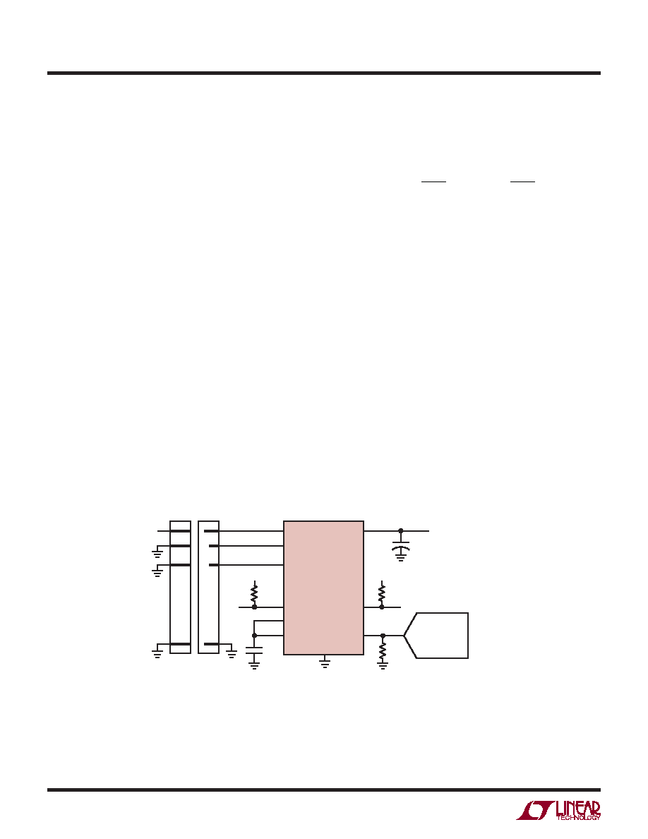
Design Example
Consider the following design example (Figure 5): VIN =
12V, IMAX = 5A. IINRUSH = 100mA, CL = 330μF, VPWRGD
= 10.5V.
The inrush current is dened by the current required to
charge the output capacitor using the xed 0.3V/ms GATE
charge up rate. The inrush current is dened as:
I
INRUSH = CL
0.3V
ms
= 330F
0.3V
ms
= 100mA
As mentioned previously, the charge up time is the out-
put voltage (12V) divided by the output rate of 0.3V/ms
resulting in 40ms. The peak power dissipation of 12V at
100mA (or 1.2W) is within the SOA of the pass MOSFET for
40ms (see MOSFET SOA curve in the Typical Performance
Characteristics section).
NextthepowerdissipatedintheMOSFETduringovercurrent
must be limited. The active current limit uses a timer to
prevent excessive energy dissipation in the MOSFET. The
worst-case power dissipation occurs when the voltage
versus current prole of the foldback current limit is at the
maximum. This occurs when the current is 6.1A and the
voltage is one half of the 12V or 6V. See the Current Limit
Sense Voltage vs FB Voltage in the Typical Performance
Characteristics section to view this prole. In order to
survive 36W, the MOSFET SOA dictates a maximum time
of 10ms (see SOA graph). Use the internal 2ms timer
invoked by tying the TIMER pin to INTVCC.
Figure 5. 5A, 12V Card Resident Application
ADC
C1
0.1μF
12V
VOUT
12V
5A
R2
20k
4219 F05
R1
10k
12V
R3
10k
12V
CL
330μF
VDD
OUT
PG
GND
IMON
LTC4219DHC-12
INTVCC
TIMER
EN1
EN2
FLT
+
相关PDF资料 |
PDF描述 |
|---|---|
| LTC4219IDHC-5#PBF | 1-CHANNEL POWER SUPPLY SUPPORT CKT, PDSO16 |
| LTC4219CDHC-5#PBF | 1-CHANNEL POWER SUPPLY SUPPORT CKT, PDSO16 |
| LTC4224CMS-1#PBF | 2-CHANNEL POWER SUPPLY SUPPORT CKT, PDSO10 |
| LTC4224CDDB-2#PBF | 2-CHANNEL POWER SUPPLY SUPPORT CKT, PDSO10 |
| LTC4224IDDB-2#PBF | 2-CHANNEL POWER SUPPLY SUPPORT CKT, PDSO10 |
相关代理商/技术参数 |
参数描述 |
|---|---|
| LTC4219IDHC-5#PBF | 功能描述:IC CONTROLLER HOT SWAP 5A 16DFN RoHS:是 类别:集成电路 (IC) >> PMIC - 热交换 系列:- 标准包装:50 系列:- 类型:热交换控制器 应用:-48V 远程电力系统,AdvancedTCA ? 系统,高可用性 内部开关:无 电流限制:可调 电源电压:11.5 V ~ 14.5 V 工作温度:-40°C ~ 85°C 安装类型:表面贴装 封装/外壳:10-TFSOP,10-MSOP(0.118",3.00mm 宽) 供应商设备封装:10-MSOP 包装:管件 |
| LTC4219IDHC-5#TRPBF | 功能描述:IC CONTROLLER HOT SWAP 5A 16DFN RoHS:是 类别:集成电路 (IC) >> PMIC - 热交换 系列:- 产品培训模块:Lead (SnPb) Finish for COTS Obsolescence Mitigation Program 标准包装:119 系列:- 类型:热交换控制器 应用:通用型,PCI Express? 内部开关:无 电流限制:- 电源电压:3.3V,12V 工作温度:-40°C ~ 85°C 安装类型:表面贴装 封装/外壳:80-TQFP 供应商设备封装:80-TQFP(12x12) 包装:托盘 产品目录页面:1423 (CN2011-ZH PDF) |
| LTC4219IDHC-5-PBF | 制造商:LINER 制造商全称:Linear Technology 功能描述:5A Integrated Hot Swap Controller |
| LTC4219IDHC-5-TRPBF | 制造商:LINER 制造商全称:Linear Technology 功能描述:5A Integrated Hot Swap Controller |
| LTC4220 | 制造商:LINER 制造商全称:Linear Technology 功能描述:Negative Voltage Hot Swap Controllers |
发布紧急采购,3分钟左右您将得到回复。