- 您现在的位置:买卖IC网 > PDF目录30772 > LTC4219IDHC-12#TRPBF (LINEAR TECHNOLOGY CORP) 1-CHANNEL POWER SUPPLY SUPPORT CKT, PDSO16 PDF资料下载
参数资料
| 型号: | LTC4219IDHC-12#TRPBF |
| 厂商: | LINEAR TECHNOLOGY CORP |
| 元件分类: | 电源管理 |
| 英文描述: | 1-CHANNEL POWER SUPPLY SUPPORT CKT, PDSO16 |
| 封装: | 5 X 3 MM, LEAD FREE, PLASTIC, MO-229WJED-1, DFN-16 |
| 文件页数: | 7/18页 |
| 文件大小: | 195K |
| 代理商: | LTC4219IDHC-12#TRPBF |
LTC4219
15
4219fb
APPLICATIONS INFORMATION
The power good threshold using the internal resistive
divider on the FB pin matches the 10.5V requirement.
The nal schematic in Figure 5 results in very few external
components. The pull-up resistors, R1 and R3, connect
to the FLT and PG pins while the 20k (R2) converts the
IMON current to a voltage at a ratio:
V
IMON = 20 A/A
20k IOUT = 0.4 V/A
IOUT
In addition there is a 0.1μF bypass (C1) on the INTVCC pin.
Layout Considerations
In Hot Swap applications where load currents can be 5A,
narrow PCB tracks exhibit more resistance than wider tracks
and operate at elevated temperatures. The minimum trace
width for 1oz copper foil is 0.02" per amp to make sure
the trace stays at a reasonable temperature. Using 0.03"
per amp or wider is recommended. Note that 1oz copper
exhibits a sheet resistance of about 0.5m
W/square. Small
resistances add up quickly in high current applications.
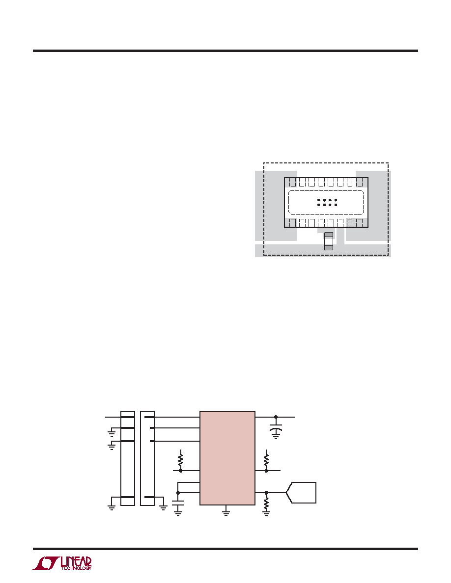
There are two VDD pins on opposite sides of the package
that connect to the sense resistor and MOSFET. The PCB
layout should be balanced and symmetrical to each VDD
pin to balance current in the MOSFET bond wires. Figure 6
shows a recommended layout for the LTC4219.
Although the MOSFET is self protected from overtem-
perature, it is recommended to solder the backside of the
package to a copper trace to provide a good heat sink.
Note that the backside is connected to the SENSE pin and
cannot be soldered to the ground plane. During normal
loads the power dissipated in the package is as high as
1.9W. A 10mm
10mm area of 1oz copper should be suf-
cient. This area of copper can be divided in many layers.
It is also important to put C1, the bypass capacitor for
the INTVCC pin as close as possible between the INTVCC
and GND.
Figure 6. Recommended Layout
4217 F06
HEAT SINK
VIA TO
SINK
GND
C
OUT
VDD
CT
0.1μF
5V
RMON
20k
4219 F07
R2
10k
5V
R1
10k
CL
100μF
VDD
EN1
EN2
OUT
PG
GND
IMON
LTC4219DHC-5
INTVCC
TIMER
FLT
+
VOUT
5V
5A
ADC
Additional Applications
The LTC4219 has a wide operating range from 2.9V to 15V.
The PG threshold is set with an internal resistive divider.
All other functions are independent of supply voltage.
Figure 7 shows a 5V application with a PG threshold of
4.35V.
In addition to Hot Swap applications, the LTC4219 also
functions as a backplane resident switch for removable
load cards (see the Typical Application section).
Figure 7. 5V, 5A Card Resident Application
相关PDF资料 |
PDF描述 |
|---|---|
| LTC4219IDHC-5#PBF | 1-CHANNEL POWER SUPPLY SUPPORT CKT, PDSO16 |
| LTC4219CDHC-5#PBF | 1-CHANNEL POWER SUPPLY SUPPORT CKT, PDSO16 |
| LTC4224CMS-1#PBF | 2-CHANNEL POWER SUPPLY SUPPORT CKT, PDSO10 |
| LTC4224CDDB-2#PBF | 2-CHANNEL POWER SUPPLY SUPPORT CKT, PDSO10 |
| LTC4224IDDB-2#PBF | 2-CHANNEL POWER SUPPLY SUPPORT CKT, PDSO10 |
相关代理商/技术参数 |
参数描述 |
|---|---|
| LTC4219IDHC-5#PBF | 功能描述:IC CONTROLLER HOT SWAP 5A 16DFN RoHS:是 类别:集成电路 (IC) >> PMIC - 热交换 系列:- 标准包装:50 系列:- 类型:热交换控制器 应用:-48V 远程电力系统,AdvancedTCA ? 系统,高可用性 内部开关:无 电流限制:可调 电源电压:11.5 V ~ 14.5 V 工作温度:-40°C ~ 85°C 安装类型:表面贴装 封装/外壳:10-TFSOP,10-MSOP(0.118",3.00mm 宽) 供应商设备封装:10-MSOP 包装:管件 |
| LTC4219IDHC-5#TRPBF | 功能描述:IC CONTROLLER HOT SWAP 5A 16DFN RoHS:是 类别:集成电路 (IC) >> PMIC - 热交换 系列:- 产品培训模块:Lead (SnPb) Finish for COTS Obsolescence Mitigation Program 标准包装:119 系列:- 类型:热交换控制器 应用:通用型,PCI Express? 内部开关:无 电流限制:- 电源电压:3.3V,12V 工作温度:-40°C ~ 85°C 安装类型:表面贴装 封装/外壳:80-TQFP 供应商设备封装:80-TQFP(12x12) 包装:托盘 产品目录页面:1423 (CN2011-ZH PDF) |
| LTC4219IDHC-5-PBF | 制造商:LINER 制造商全称:Linear Technology 功能描述:5A Integrated Hot Swap Controller |
| LTC4219IDHC-5-TRPBF | 制造商:LINER 制造商全称:Linear Technology 功能描述:5A Integrated Hot Swap Controller |
| LTC4220 | 制造商:LINER 制造商全称:Linear Technology 功能描述:Negative Voltage Hot Swap Controllers |
发布紧急采购,3分钟左右您将得到回复。