- 您现在的位置:买卖IC网 > PDF目录19841 > LTC4221CGN#PBF (Linear Technology)IC CTLR HOT SWAP DUAL 16SSOP PDF资料下载
参数资料
| 型号: | LTC4221CGN#PBF |
| 厂商: | Linear Technology |
| 文件页数: | 14/28页 |
| 文件大小: | 272K |
| 描述: | IC CTLR HOT SWAP DUAL 16SSOP |
| 标准包装: | 100 |
| 类型: | 热交换控制器 |
| 应用: | 通用 |
| 内部开关: | 无 |
| 电源电压: | 1 V ~ 13.5 V |
| 工作温度: | 0°C ~ 70°C |
| 安装类型: | 表面贴装 |
| 封装/外壳: | 16-SSOP(0.154",3.90mm 宽) |
| 供应商设备封装: | 16-SSOP |
| 包装: | 管件 |
| 产品目录页面: | 1342 (CN2011-ZH PDF) |
第1页第2页第3页第4页第5页第6页第7页第8页第9页第10页第11页第12页第13页当前第14页第15页第16页第17页第18页第19页第20页第21页第22页第23页第24页第25页第26页第27页第28页
14
LTC4221
4221fa
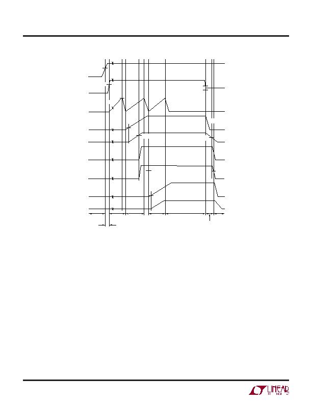
sequential power up from time points 4 to 8 and a
sequential power-down programmed from time points 9
to 11. To achieve this the circuit requires the functionality
of the PWRGD1 pin and will be featured in the next section.
The circuit in Figure 2a sits on a daughter board with
staggered pins on its edge connectors. Supply voltage and
ground connections are wired to long-edge connector
pins while both ON pins are connected to a short-edge
connector pin through a resistive divider. Until the con-
nectors are fully mated, ON1 is pulled low and holds both
channels in the reset state. When the connectors have
properly seated, the ON pins are pulled above 0.851V and
an initial timing cycle starts. This cycle is restarted by any
transitions on the ON pins across their off thresholds and
adds a further delay for the plug-in transients to die off
before allowing a start-up cycle. The Typical Application
circuit on the first page of this data sheet shows similar
considerations in the design of its PCB edge connectors,
and the resistive dividers connected to ON1 and ON2 act
as an external UVLO to override the internal one. An RC
filter can be added at the ON1 pin to increase the delay time
at card insertion to allow bus supply transients to stabilize.
FB and PWRGD Pin Functions
Each FB pin is used to detect undervoltage and overvoltage
in its channel output voltage (V
OUT
) through a resistive
divider. Each FB pin has an undervoltage comparator with
a high-to-low threshold of 0.617V and 3mV hysteresis.
The output of this comparator controls the channels
open-drain PWRGD output. During UVLO, both PWRGD
pins are pulled low by internal N-channel MOSFET pull-
downs. As both channels come out of UVLO, control of
PWRGD1 is passed to FB1and control of PWRGD2 to FB2.
Each PWRGD pin can be connected to a pull-up resistor to
0.821V
100糀
V
CCn
1 2
3 4
5 6 7
8
9 1011
ON1
TIMER
GATE1
V
OUT1
PWRGD1
ON2
GATE2
UVLO
INITIAL
TIMING
RESET
V
OUT2
V
CCn(UVL)
0.851V
0.821V
0.4V
1.234V
20糀
100糀
DISCHARGE
BY LOAD
DISCHARGE
BY LOAD
4221 F03
20糀
9.5糀
9.5糀
V
TH
0.851V
V
TH
V
FB1
= 0.620V
V
FB1
= 0.617V
CHANNEL 1
START-UP
CHANNEL 2
START-UP
CHANNEL 1 OFF
CHANNEL 2 NORMAL
NORMAL
OFF
1.9糀
APPLICATIO S I FOR ATIO
U
U
U
Figure 3. Sequential Power On/Off Timing Waveforms
相关PDF资料 |
PDF描述 |
|---|---|
| 7-1734857-5 | PCI EXP STRADDLE 98P BLK 30U" |
| GSC49DRYN | CONN EDGECARD 98POS DIP .100 SLD |
| LTM8052IV#PBF | IC UMODULE CVCC STEP DOWN 81LGA |
| VE-JW3-CW-B1 | CONVERTER MOD DC/DC 24V 100W |
| GMM36DTBN-S664 | CONN EDGECARD 72POS R/A .156 |
相关代理商/技术参数 |
参数描述 |
|---|---|
| LTC4221IGN | 功能描述:IC CTRLR HOTSWAP DUAL 16SSOP RoHS:否 类别:集成电路 (IC) >> PMIC - 热交换 系列:- 产品培训模块:Obsolescence Mitigation Program 标准包装:100 系列:- 类型:热插拔开关 应用:通用 内部开关:是 电流限制:可调 电源电压:9 V ~ 13.2 V 工作温度:-40°C ~ 150°C 安装类型:表面贴装 封装/外壳:10-WFDFN 裸露焊盘 供应商设备封装:10-TDFN-EP(3x3) 包装:管件 |
| LTC4221IGN#PBF | 功能描述:IC CTRLR HOTSWAP DUAL 16SSOP RoHS:否 类别:集成电路 (IC) >> PMIC - 热交换 系列:- 产品培训模块:Obsolescence Mitigation Program 标准包装:100 系列:- 类型:热插拔开关 应用:通用 内部开关:是 电流限制:可调 电源电压:9 V ~ 13.2 V 工作温度:-40°C ~ 150°C 安装类型:表面贴装 封装/外壳:10-WFDFN 裸露焊盘 供应商设备封装:10-TDFN-EP(3x3) 包装:管件 |
| LTC4221IGN#TR | 功能描述:IC CTRLR HOTSWAP DUAL 16SSOP RoHS:否 类别:集成电路 (IC) >> PMIC - 热交换 系列:- 产品培训模块:Obsolescence Mitigation Program 标准包装:100 系列:- 类型:热插拔开关 应用:通用 内部开关:是 电流限制:可调 电源电压:9 V ~ 13.2 V 工作温度:-40°C ~ 150°C 安装类型:表面贴装 封装/外壳:10-WFDFN 裸露焊盘 供应商设备封装:10-TDFN-EP(3x3) 包装:管件 |
| LTC4221IGN#TRPBF | 功能描述:IC CTRLR HOTSWAP DUAL 16SSOP RoHS:是 类别:集成电路 (IC) >> PMIC - 热交换 系列:- 产品培训模块:Obsolescence Mitigation Program 标准包装:100 系列:- 类型:热插拔开关 应用:通用 内部开关:是 电流限制:可调 电源电压:9 V ~ 13.2 V 工作温度:-40°C ~ 150°C 安装类型:表面贴装 封装/外壳:10-WFDFN 裸露焊盘 供应商设备封装:10-TDFN-EP(3x3) 包装:管件 |
| LTC4222 | 制造商:LINER 制造商全称:Linear Technology 功能描述:Dual Hot Swap Controller |
发布紧急采购,3分钟左右您将得到回复。