- 您现在的位置:买卖IC网 > PDF目录20107 > LTC4225IUFD-2#PBF (Linear Technology)IC CONTROLLER HOT SWAP 24-QFN PDF资料下载
参数资料
| 型号: | LTC4225IUFD-2#PBF |
| 厂商: | Linear Technology |
| 文件页数: | 18/24页 |
| 文件大小: | 346K |
| 描述: | IC CONTROLLER HOT SWAP 24-QFN |
| 标准包装: | 73 |
| 类型: | 热交换控制器 |
| 应用: | 通用 |
| 内部开关: | 无 |
| 电流限制: | 可调 |
| 电源电压: | 2.9 V ~ 18 V |
| 工作温度: | -40°C ~ 85°C |
| 安装类型: | 表面贴装 |
| 封装/外壳: | 24-WFQFN 裸露焊盘 |
| 供应商设备封装: | 24-QFN(5x4) |
| 包装: | 管件 |
LTC4225-1/LTC4225-2
18
422512f
applicaTions inForMaTion
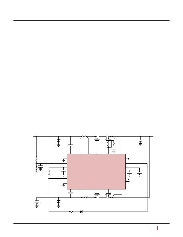
Power Prioritizer
Figure 8 shows an application where either of two supplies
is passed to the output on the basis of priority, rather than
simply allowing the highest voltage to prevail. The 5V pri-
mary supply (INPUT 1) is passed to the output whenever
it is available; power is drawn from the 12V backup supply
(INPUT 2) only when the primary supply is unavailable. As
long as INPUT 1 is above the 4.3V UV threshold set by the
R1-R2 divider at the ON1 pin, M
H1
is turned on connecting
INPUT 1 to the output. When M
H1
is on, PWRGD1 goes
low, which in turn pulls ON2 low and disables the IN2
path by turning M
H2
off. If the primary supply fails and
INPUT? drops below 4.3V , ON1 turns off M
H1
and PWRGD1
goes high, allowing ON2 to turn on M
H2
and connect the
INPUT 2 to the output. Diode D1 ensures that ON2 remains
above 0.6V while in the off state so that when ON2 goes
high, M
H2
is turned on immediately without invoking the
100ms turn-on delay. When INPUT 1 returns to a viable
voltage, M
H1
turns on and M
H2
turns off. The ideal diode
MOSFETs M
D1
and M
D2
prevent backfeeding of one input
to the other under any condition.
Additional Applications
In most applications, the back-to-back MOSFETs are con-
fgured with the MOSFET on the supply side as the ideal
diode and the MOSFET on the load side as the Hot Swap
control. But for some applications, the arrangement of the
MOSFETs for the ideal diode and the Hot Swap control may
reversed as shown in Figure 9. The Hot Swap MOSFET is
placed on the supply side and the ideal diode MOSFET on
the load side with the source terminals connected together.
If this configuration is operated with 12V supplies, the
gate-to-source breakdown voltage of the MOSFETs can
be exceeded when the input or output is connected to
ground as the LTC4225s internal 12V clamps only limit
the DGATE-to-IN and HGATE-to-OUT pin voltages. Choose
a MOSFET whose gate-to-source breakdown voltage is
rated for 25V or more as 24V voltage can appear across
the GATE and SOURCE pins of the MOSFET during an
input or output short. As shown in Figure 9, if a MOSFET
with a lower rated gate-to-source breakdown voltage is
chosen, an external Zener diode clamp is required between
the GATE and SOURCE pins of the MOSFET to prevent it
from breaking down.
Figure 8. 2-Channel Power Prioritizer
CPO1
ON1
EN1
ON2
EN2
INTV
CC
GND
C
CP1
0.1礔
C1
0.1礔
C
F1
0.1礔
C
HG1
33nF
C
L
470礔
C
T2
47nF
Z1
SMAJ13A
INPUT 1
INPUT 2
5V
PRIMARY
SUPPLY
12V
BACKUP
SUPPLY
C
CP2
0.1礔
C
T1
47nF
IN1
SENSE1 DGATE1
M
D1
SiR466DP
M
H1
SiR466DP
LTC4225
R
S1
0.006
M
D2
SiR466DP
M
H2
SiR466DP
R
S2
0.006
R3
3.92k
D1
LS4148
HGATE1
R
H1
10
R
HG1
47
V
OUT
5A
OUT1
CPO2
IN2
SENSE2 DGATE2
HGATE2
OUT2
422512 F08
FAULT1
PWRGD2
FAULT2
Z2
SMAJ13A
R4
41.2k
R2
49.9k
R1
20k
PWRGD1
TMR1
TMR2
+
+
相关PDF资料 |
PDF描述 |
|---|---|
| VI-27P-CX | CONVERTER MOD DC/DC 13.8V 75W |
| T86C155K035EAAS | CAP TANT 1.5UF 35V 10% 2312 |
| VI-27N-CX | CONVERTER MOD DC/DC 18.5V 75W |
| CENB1010A1803F01 | POWER SUPPLY EXT 12W 18V @ 0.67A |
| TCJC336M010R0100 | CAP TANT 33UF 10V 20% 2312 |
相关代理商/技术参数 |
参数描述 |
|---|---|
| LTC4226 | 制造商:LINER 制造商全称:Linear Technology 功能描述:Wide Operating Range Dual Hot Swap Controller Fast Response Limits Peak Fault Current |
| LTC4226CMS-1#PBF | 制造商:Linear Technology 功能描述:Hot Swap Controller 2-CH 44V 16-Pin MSOP 制造商:Linear Technology 功能描述:IC HOT SWAP CONTROL DUAL 16MSOP |
| LTC4226CMS-1#TRPBF | 制造商:Linear Technology 功能描述:Hot Swap Controller 2-CH 44V 16-Pin MSOP T/R 制造商:Linear Technology 功能描述:IC HOT SWAP CONTROL DUAL 16MSOP |
| LTC4226CMS-2#PBF | 制造商:Linear Technology 功能描述:Hot Swap Controller 2-CH 44V 16-Pin MSOP 制造商:Linear Technology 功能描述:IC HOT SWAP CONTROL DUAL 16MSOP |
| LTC4226CMS-2#TRPBF | 制造商:Linear Technology 功能描述:Hot Swap Controller 2-CH 44V 16-Pin MSOP T/R 制造商:Linear Technology 功能描述:IC HOT SWAP CONTROL DUAL 16MSOP |
发布紧急采购,3分钟左右您将得到回复。