- 您现在的位置:买卖IC网 > PDF目录11577 > LTC4267CGN#TRPBF (Linear Technology)IC POE 802.3AF INTERFACE 16SSOP PDF资料下载
参数资料
| 型号: | LTC4267CGN#TRPBF |
| 厂商: | Linear Technology |
| 文件页数: | 5/32页 |
| 文件大小: | 0K |
| 描述: | IC POE 802.3AF INTERFACE 16SSOP |
| 标准包装: | 2,500 |
| 控制器类型: | 以太网供电控制器(POE) |
| 接口: | IEEE 802.3af |
| 电流 - 电源: | 3mA |
| 工作温度: | 0°C ~ 70°C |
| 安装类型: | 表面贴装 |
| 封装/外壳: | 16-SSOP(0.154",3.90mm 宽) |
| 供应商设备封装: | 16-SSOP |
| 包装: | 带卷 (TR) |
| 相关产品: | 732-2437-6-ND - TRANS FLYBACK POE 40UH SMD 732-2436-6-ND - TRANS FLYBACK POE 35UH SMD 732-2435-6-ND - TRANS FLYBACK POE 127UH SMD 732-2434-6-ND - TRANS FLYBACK POE 127UH SMD 732-2433-6-ND - TRANS FLYBACK POE 127UH SMD 732-2432-6-ND - TRANS FLYBACK POE 127UH SMD 732-2431-6-ND - TRANS FLYBACK POE 127UH SMD 732-2430-6-ND - TRANS FLYBACK POE 127UH SMD 732-2437-1-ND - TRANS FLYBACK POE 40UH SMD 732-2436-1-ND - TRANS FLYBACK POE 35UH SMD 更多... |
第1页第2页第3页第4页当前第5页第6页第7页第8页第9页第10页第11页第12页第13页第14页第15页第16页第17页第18页第19页第20页第21页第22页第23页第24页第25页第26页第27页第28页第29页第30页第31页第32页
LTC4267
13
4267fc
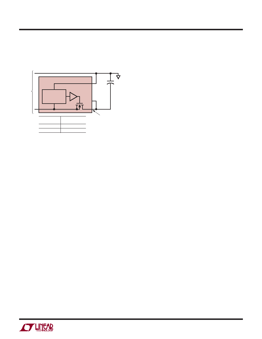
Figure 5. LTC4267 VPORTN Undervoltage Lockout
the classication current is reenabled. C1 will discharge
through the PD circuitry and the POUT pin will go to a high
impedance state.
limit because the load capacitor is charged with a current
below the IEEE inrush current limit specication.
As the LTC4267 switches from the low to high level current
limit, the current will increase momentarily. This current
spike is a result of the LTC4267 charging the last 1.5V at
the high level current limit. When charging a 10F capaci-
tor, the current spike is typically 100s wide and 125%
of the nominal low level current limit.
The LTC4267 stays in the high level current limit mode
until the input voltage drops below the UVLO turn-off
threshold. This dual level current limit provides the sys-
tem designer with the exibility to design PDs which are
compatible with legacy PSEs while also being able to take
advantage of the higher power allocation available in an
IEEE 802.3af system.
During the current limited turn on, a large amount of
power is dissipated in the power MOSFET. The LTC4267
PD interface is designed to accept this thermal load and
is thermally protected to avoid damage to the onboard
power MOSFET. Note that in order to adhere to the IEEE
802.3af standard, it is necessary for the PD designer to
ensure the PD steady state power consumption falls within
the limits shown in Table 2. In addition, the steady state
current must be less than ILIM_HI.
Power Good
The LTC4267 PD Interface includes a power good circuit
(Figure 6) that is used to indicate that load capacitor C1
is fully charged and that the switching regulator can start
operation. The power good circuit monitors the voltage
across the internal UVLO power MOSFET and PWRGD is
asserted when the voltage falls below 1.5V. The power
good circuit includes hysteresis to allow the LTC4267 to
operate near the current limit point without inadvertently
disabling PWRGD. The MOSFET voltage must increase to
3V before PWRGD is disabled.
If a sudden increase in voltage appears on the input line,
this voltage step will be transferred through capacitor C1
and appear across the power MOSFET. The response of
the LTC4267 will depend on the magnitude of the voltage
step, the rise time of the step, the value of capacitor C1
and the switching regulator load. For fast rising inputs,
APPLICATIO S I FOR ATIO
WU
UU
Input Current Limit
IEEE 802.3af species a maximum inrush current and also
species a minimum load capacitor between the VPORTP
and POUT pins. To control turn-on surge current in the
system, the LTC4267 integrates a dual level current limit
circuit with an onboard power MOSFET and sense resis-
tor to provide a complete inrush control circuit without
additional external components. At turn-on, the LTC4267
will limit the input current to the low level, allowing the
load capacitor to ramp up to the line voltage in a controlled
manner.
The LTC4267 has been specically designed to interface
with legacy PSEs which do not meet the inrush current
requirement of the IEEE 802.3af specication. At turn-on
the LTC4267 current limit is set to the lower level. After C1
is charged up and the POUT – VPORTN voltage difference is
below the power good threshold, the LTC4267 switches
to the high level current limit. The dual level current limit
allows legacy PSEs with limited current sourcing capability
to power up the PD while also allowing the PD to draw full
power from an IEEE 802.3af PSE. The dual level current
limit also allows use of arbitrarily large load capacitors.
The IEEE 802.3af specication mandates that at turn-on
the PD not exceed the inrush current limit for more than
50ms. The LTC4267 is not restricted to the 50ms time
C1
5F
MIN
VPORTN
VPORTP
POUT
PGND
LTC4267
4267 F05
TO
PSE
UNDERVOLTAGE
LOCKOUT
CIRCUIT
CURRENT-LIMITED
TURN ON
+
INPUT
LTC4267
VOLTAGE
POWER MOSFET
0V TO UVLO*
OFF
>UVLO*
ON
*UVLO INCLUDES HYSTERESIS
RISING INPUT THRESHOLD
–36V
FALLING INPUT THRESHOLD
–30.5V
相关PDF资料 |
PDF描述 |
|---|---|
| 031-4237 | CONN BNC RCPT BULKHEAD REAR MNT |
| VI-2NJ-CV-S | CONVERTER MOD DC/DC 36V 150W |
| VI-2NF-CV-S | CONVERTER MOD DC/DC 72V 150W |
| 083-59SP | CONN PLUG UHF CRIMP RG59,140 |
| VI-2N4-CV-S | CONVERTER MOD DC/DC 48V 150W |
相关代理商/技术参数 |
参数描述 |
|---|---|
| LTC4267IDHC | 制造商:Linear Technology 功能描述:Hot Swap Controller 1-CH -57V 16-Pin DFN EP |
| LTC4267IDHC#PBF | 功能描述:IC POE 802.3AF INTERFACE 16-DFN RoHS:是 类别:集成电路 (IC) >> 接口 - 控制器 系列:- 标准包装:2,450 系列:- 控制器类型:SPI 总线至 I²C 总线桥接 接口:I²C,串行,SPI 电源电压:2.4 V ~ 3.6 V 电流 - 电源:11mA 工作温度:-40°C ~ 85°C 安装类型:表面贴装 封装/外壳:24-VFQFN 裸露焊盘 供应商设备封装:24-HVQFN(4x4) 包装:托盘 配用:568-3511-ND - DEMO BOARD SPI TO I2C 其它名称:935286452157SC18IS600IBSSC18IS600IBS-ND |
| LTC4267IDHC#TRPBF | 功能描述:IC POE 802.3AF INTERFACE 16-DFN RoHS:是 类别:集成电路 (IC) >> 接口 - 控制器 系列:- 标准包装:2,450 系列:- 控制器类型:SPI 总线至 I²C 总线桥接 接口:I²C,串行,SPI 电源电压:2.4 V ~ 3.6 V 电流 - 电源:11mA 工作温度:-40°C ~ 85°C 安装类型:表面贴装 封装/外壳:24-VFQFN 裸露焊盘 供应商设备封装:24-HVQFN(4x4) 包装:托盘 配用:568-3511-ND - DEMO BOARD SPI TO I2C 其它名称:935286452157SC18IS600IBSSC18IS600IBS-ND |
| LTC4267IDHC-1#PBF | 制造商:Linear Technology 功能描述:Bulk |
| LTC4267IDHC-3#PBF | 功能描述:IC POE 802.3AF W/REG 16-DFN RoHS:是 类别:集成电路 (IC) >> 接口 - 控制器 系列:- 标准包装:2,450 系列:- 控制器类型:SPI 总线至 I²C 总线桥接 接口:I²C,串行,SPI 电源电压:2.4 V ~ 3.6 V 电流 - 电源:11mA 工作温度:-40°C ~ 85°C 安装类型:表面贴装 封装/外壳:24-VFQFN 裸露焊盘 供应商设备封装:24-HVQFN(4x4) 包装:托盘 配用:568-3511-ND - DEMO BOARD SPI TO I2C 其它名称:935286452157SC18IS600IBSSC18IS600IBS-ND |
发布紧急采购,3分钟左右您将得到回复。