- 您现在的位置:买卖IC网 > PDF目录44997 > LTC4365CTS8#TRMPBF (LINEAR TECHNOLOGY CORP) 1-CHANNEL POWER SUPPLY SUPPORT CKT, PDSO8 PDF资料下载
参数资料
| 型号: | LTC4365CTS8#TRMPBF |
| 厂商: | LINEAR TECHNOLOGY CORP |
| 元件分类: | 电源管理 |
| 英文描述: | 1-CHANNEL POWER SUPPLY SUPPORT CKT, PDSO8 |
| 封装: | LEAD FREE, PLASTIC, MO-193, TSOT-23, 8 PIN |
| 文件页数: | 6/16页 |
| 文件大小: | 369K |
| 代理商: | LTC4365CTS8#TRMPBF |
LTC4365
14
4365f
APPLICATIONS INFORMATION
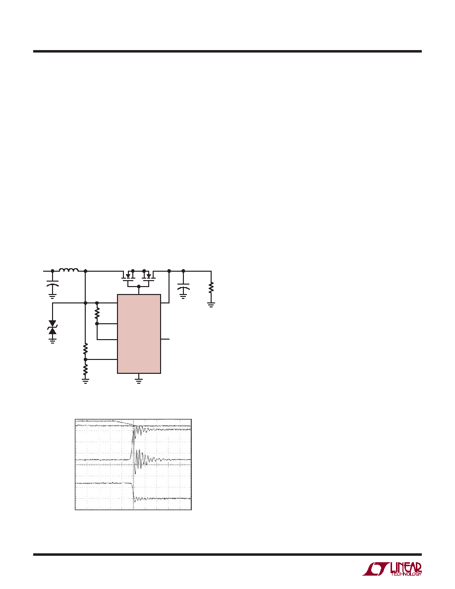
Transients During OV Fault
The circuit of Figure 14 was used to display transients
during an overvoltage condition. The nominal input supply
is 24V and it has an overvoltage threshold of 30V. The
parasitic inductance is that of a 1 foot wire (roughly 300nH).
Figure 15 shows the waveforms during an overvoltage
condition at VIN. These transients depend on the parasitic
inductance and resistance of the wire along with the ca-
pacitance at the VIN node. D1 is an optional power clamp
(TVS, Tranzorb) recommended for applications where
the DC input voltage can exceed 24V and with large VIN
parasitic inductance. No clamp was used to capture the
waveforms of Figure 15. In order to maintain reverse supply
protection, D1 must be a bi-directional clamp rated for at
least 225W peak pulse power dissipation.
MOSFET Selection
To protect against a negative voltage at VIN, the external
N-channel MOSFETs must be configured in a back-to-
back arrangement. Dual N-channel packages are thus the
best choice. The MOSFET is selected based on its power
handling capability, drain and gate breakdown voltages,
and threshold voltage.
The drain to source breakdown voltage must be higher
than the maximum voltage expected between VIN and
VOUT. Note that if an application generates high energy
transients during normal operation or during Hot Swap,
the external MOSFET must be able to withstand this
transient voltage.
Due to the high impedance nature of the charge pump that
drives the GATE pin, the total leakage on the GATE pin must
be kept low. The gate drive curves of Figure 2 were measured
with a 1μA load on the GATE pin. Therefore, the leakage
on the GATE pin must be no greater than 1μA in order to
match the curves of Figure 2. Higher leakage currents will
result in lower gate drive. The dual N-channel MOSFETs
shown in Table 1 all have a maximum GATE leakage cur-
rent of 100nA. Additionally, Table 1 lists representative
MOSFETs that would work at different values of VIN.
Layout Considerations
The trace length between the VIN pin and the drain of the
external MOSFET should be minimized, as well as the
trace length between the GATE pin of the LTC4365 and
the gates of the external MOSFETs.
Place the bypass capacitors at VOUT as close as possible
to the external MOSFET. Use high frequency ceramic
capacitors in addition to bulk capacitors to mitigate Hot
Swap ringing. Place the high frequency capacitors closest
to the MOSFET. Note that bulk capacitors mitigate ringing
by virtue of their ESR. Ceramic capacitors have low ESR
and can thus ring near their resonant frequency.
VIN
UV
OV
SHDN
OV = 30V
4365 F14
VOUT
FAULT
GATE
M1
M2
VIN
24V
SI9945
60V
12 INCH WIRE
LENGTH
VOUT
GND
LTC4365
R2
2370k
R1
40.2k
R3
100k
COUT
100μF
+
CIN
1000μF
D1
OPTIONAL
+
9Ω
2A/DIV
GND
0A
20V/DIV
4365 F15
250ns/DIV
GATE
VOUT
VIN
IIN
GATE
VOUT
Figure 14. OV Fault with Large VIN Inductance
Figure 15. Transients During OV Fault When No
Tranzorb (TVS) Is Used
相关PDF资料 |
PDF描述 |
|---|---|
| LTC4365HDDB#TRMPBF | 1-CHANNEL POWER SUPPLY SUPPORT CKT, PDSO8 |
| LTC4365HDDB#TRPBF | 1-CHANNEL POWER SUPPLY SUPPORT CKT, PDSO8 |
| LTC4365HTS8#TRMPBF | 1-CHANNEL POWER SUPPLY SUPPORT CKT, PDSO8 |
| LTC4365ITS8#TRPBF | 1-CHANNEL POWER SUPPLY SUPPORT CKT, PDSO8 |
| LTC4412IHVS6#TRM | 1-CHANNEL POWER SUPPLY SUPPORT CKT, PDSO6 |
相关代理商/技术参数 |
参数描述 |
|---|---|
| LTC4365HDDB#PBF | 制造商:Linear Technology 功能描述:Bulk 制造商:Linear Technology 功能描述:PROTECTION CONTROLLER 2.5V TO 制造商:Linear Technology 功能描述:PROTECTION CONTROLLER, 2.5V TO 34V, DFN-8; Controller Applications:Automotive, Industrial Automation, Laptops, Portable Instrumentation; Internal Switch:No; Supply Voltage Min:2.5V; Supply Voltage Max:34V; Digital IC Case Style:DFN ;RoHS Compliant: Yes |
| LTC4365HDDB#TRMPBF | 功能描述:IC OVERVOLTAGE PROTECT 8-DFN RoHS:是 类别:集成电路 (IC) >> PMIC - 电源管理 - 专用 系列:- 标准包装:1 系列:- 应用:手持/移动设备 电流 - 电源:- 电源电压:3 V ~ 5.5 V 工作温度:-40°C ~ 85°C 安装类型:表面贴装 封装/外壳:14-WFDFN 裸露焊盘 供应商设备封装:14-LLP-EP(4x4) 包装:Digi-Reel® 配用:LP3905SD-30EV-ND - BOARD EVALUATION LP3905SD-30 其它名称:LP3905SD-30DKR |
| LTC4365HDDB#TRPBF | 功能描述:IC OVERVOLTAGE PROTECT 8-DFN RoHS:是 类别:集成电路 (IC) >> PMIC - 电源管理 - 专用 系列:- 标准包装:1 系列:- 应用:手持/移动设备 电流 - 电源:- 电源电压:3 V ~ 5.5 V 工作温度:-40°C ~ 85°C 安装类型:表面贴装 封装/外壳:14-WFDFN 裸露焊盘 供应商设备封装:14-LLP-EP(4x4) 包装:Digi-Reel® 配用:LP3905SD-30EV-ND - BOARD EVALUATION LP3905SD-30 其它名称:LP3905SD-30DKR |
| LTC4365HDDB-1#TRMPBF | 制造商:Linear Technology 功能描述:IC OVERVOLTAGE PROTECT 8-DFN 制造商:Linear Technology 功能描述:IC, SUPPLY PROTECTION CONTROL, DFN-8 制造商:Linear Technology 功能描述:OV, UV & REVERSE CONTROLLER, DFN-8, Brief Features:-, Supply Voltage Min:2.5V, Supply Voltage Max:34V, Operating Temperature Min:-40C, Operating Temperature Max:125C, Digital IC Case Style:DFN, No. of Pins:8, Package / Case:8-DFN |
| LTC4365HDDB-1#TRPBF | 制造商:Linear Technology 功能描述:IC OVERVOLTAGE PROTECT 8-DFN 制造商:Linear Technology 功能描述:OV, UV & REVERSE CONTROLLER, DFN-8, Brief Features:-, Supply Voltage Min:2.5V, Supply Voltage Max:34V, Operating Temperature Min:-40C, Operating Temperature Max:125C, Digital IC Case Style:DFN, No. of Pins:8, Package / Case:8-DFN |
发布紧急采购,3分钟左右您将得到回复。