参数资料
| 型号: | LTC6403IUD-1#PBF |
| 厂商: | Linear Technology |
| 文件页数: | 20/20页 |
| 文件大小: | 0K |
| 描述: | IC AMP/DRIVER LN LP 16-QFN |
| 标准包装: | 121 |
| 类型: | ADC 驱动器 |
| 应用: | 数据采集 |
| 安装类型: | 表面贴装 |
| 封装/外壳: | 16-WFQFN 裸露焊盘 |
| 供应商设备封装: | 16-QFN-EP(3x3) |
| 包装: | 管件 |
| 产品目录页面: | 1323 (CN2011-ZH PDF) |
LTC6403-1
9
64031fa
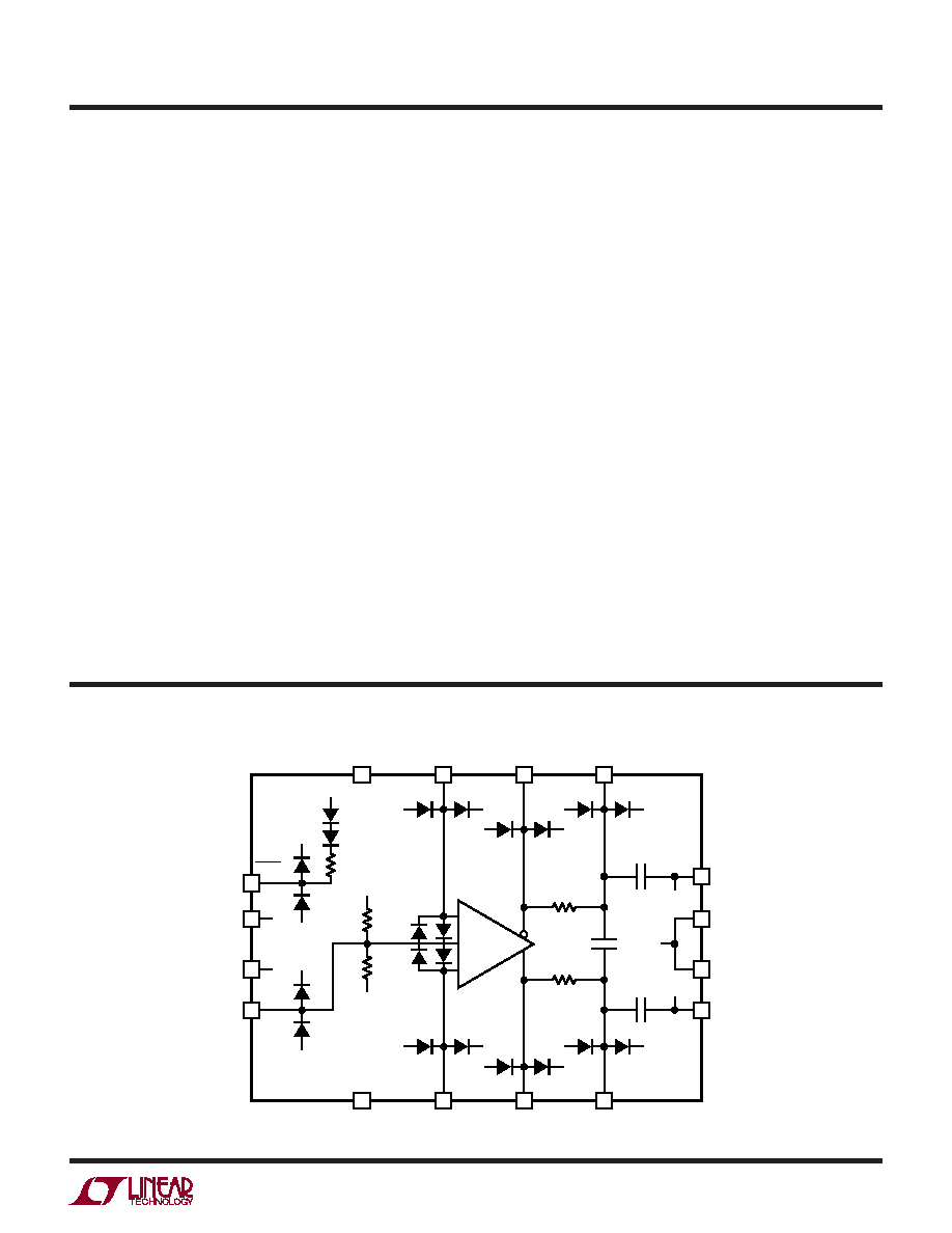
PIN FUNCTIONS
VOCM (Pin 4): Output Common Mode Reference Voltage.
The voltage on VOCMsetstheoutputcommonmodevoltage
level (which is dened as the average of the voltages on
the +OUT and –OUT pins). The VOCM pin is the midpoint
of an internal resistive voltage divider between V+ and
V– that develops a (default) mid-supply voltage potential
to maximize output signal swing. The VOCM pin can be
overdriven by an external voltage reference capable of
driving the input impedance presented by the VOCM pin.
On the LTC6403-1, the VOCM pin has an input resistance
of approximately 23k to a mid-supply potential. The VOCM
pin should be bypassed with a high quality ceramic bypass
capacitor of at least 0.01μF, (unless you are using split
supplies, then connect directly to a low impedance, low
noise ground plane) to minimize common mode noise
from being converted to differential noise by impedance
mismatches both external and internal to the IC.
NC (Pins 5, 16): No Connection. These pins are not con-
nected internally.
+OUT, –OUT (Pins 7, 14): Unltered Output Pins. Each
amplier output is designed to drive a load capacitance of
10pF. This means the amplier can drive 10pF from each
output to ground or 5pF differentially. Larger capacitive
loads should be decoupled with at least 25
Ω resistors
from each output.
+OUTF, –OUTF (Pins 8, 13): Filtered Output Pins. These
pins have a series 100
Ω resistor connected between the
ltered and unltered outputs and three 12pF capacitors.
Both +OUTF, and –OUTF have 12pF to V–, plus an additional
12pF differentially between +OUTF and –OUTF. This lter
creates a differential lowpass pole with a –3dB bandwidth
of 44.2MHz.
+IN, –IN (Pins 15, 6): Noninverting and Inverting Input
pins of the amplier, respectively. For best performance,
it is highly recommended that stray capacitance be kept
to an absolute minimum by keeping printed circuit con-
nections as short as possible and stripping back nearby
surrounding ground plane away from these pins.
Exposed Pad (Pin 17): Tie the pad to V– (Pins 3, 9, and 12).
If split supplies are used, do not tie the pad to ground.
BLOCK DIAGRAM
–
+
1
5
NC
6
–IN
7
+OUT
8
+OUTF
16
NC
15
+IN
14
–OUT
13
–OUTF
2
V+
3
V–
V+
V–
V+
100
Ω
12pF
66k
V–
4
VOCM
12
V–
64031 BD
11
V+
10
V+
9
V–
100
Ω
46k
V–
V+
V–
V+
V–
V+
V–
V+
V–
V+
V–
46k
SHDN
相关PDF资料 |
PDF描述 |
|---|---|
| AD9744ARURL7 | IC DAC 14BIT 210MSPS 28-TSSOP |
| LT6109HMS-2#PBF | IC AMP CURRENT SENSE 10-MSOP |
| LTC6403CUD-1#PBF | IC AMP/DRIVER LN LP 16-QFN |
| 74AHC1G14GV,125 | IC SCHMITT-TRG INV GATE SOT-753 |
| 74HC1G00GV,125 | IC 2-INPUT NAND GATE SC-74A |
相关代理商/技术参数 |
参数描述 |
|---|---|
| LTC6403IUD-1-TRPBF | 制造商:LINER 制造商全称:Linear Technology 功能描述:200MHz, Low Noise, Low Power Fully Differential Input/Output Amplifi er/Driver |
| LTC6404 | 制造商:LINER 制造商全称:Linear Technology 功能描述:600MHz, Low Noise, High Precision Fully Differential Input/Output Amplifi er/Driver |
| LTC6404-1 | 制造商:LINER 制造商全称:Linear Technology 功能描述:16-Bit, 20Msps ADC |
| LTC6404-2 | 制造商:LINER 制造商全称:Linear Technology 功能描述:2.7GHz, 5V, Low Noise,Rail-to-Rail Input Differential Amplifier/Driver |
| LTC6404-4 | 制造商:LINER 制造商全称:Linear Technology 功能描述:2.7GHz, 5V, Low Noise,Rail-to-Rail Input Differential Amplifier/Driver |
发布紧急采购,3分钟左右您将得到回复。