参数资料
| 型号: | LTC6403IUD-1#PBF |
| 厂商: | Linear Technology |
| 文件页数: | 4/20页 |
| 文件大小: | 0K |
| 描述: | IC AMP/DRIVER LN LP 16-QFN |
| 标准包装: | 121 |
| 类型: | ADC 驱动器 |
| 应用: | 数据采集 |
| 安装类型: | 表面贴装 |
| 封装/外壳: | 16-WFQFN 裸露焊盘 |
| 供应商设备封装: | 16-QFN-EP(3x3) |
| 包装: | 管件 |
| 产品目录页面: | 1323 (CN2011-ZH PDF) |
LTC6403-1
12
64031fa
APPLICATIONS INFORMATION
the non-linear capacitance, the outputs still have the ability
to sink and source small amounts of transient current if
exposed to signicant voltage transients. The inputs (+IN
and –IN) appear as anti-parallel diodes which can conduct
if voltage transients at the input exceed 1.4V. The inputs
also have steering diodes to either supply. The turn-on
time between the shutdown and active states is typically
4μs, and turn-off time is typically 350ns.
General Amplier Applications
As levels of integration have increased and correspond-
ingly, system supply voltages decreased, there has been
a need for ADCs to process signals differentially in order
to maintain good signal to noise ratios. These ADCs are
typically operated from a single supply voltage which can
be as low as 3V (2.7V min), and will have an optimal com-
mon mode input range near mid-supply. The LTC6403-1
makes interfacing to these ADCs trivial, by providing both
single ended to differential conversion as well as common
mode level shifting. The front page of this datasheet shows
a typical application. Referring to Figure 1, the gain to
VOUTDIFF from VINM and VINP is:
VV
V
R
VV
OUTDIFF
OUT
F
I
INP
INM
=≈
()
+
–
Note from the above equation, the differential output
voltage (V+OUT – V–OUT) is completely independent of
input and output common mode voltages. This makes
the LTC6403-1 ideally suited for pre-amplication, level
shifting and conversion of single-ended input signals to
differential output signals in preparation for driving dif-
ferential input ADCs.
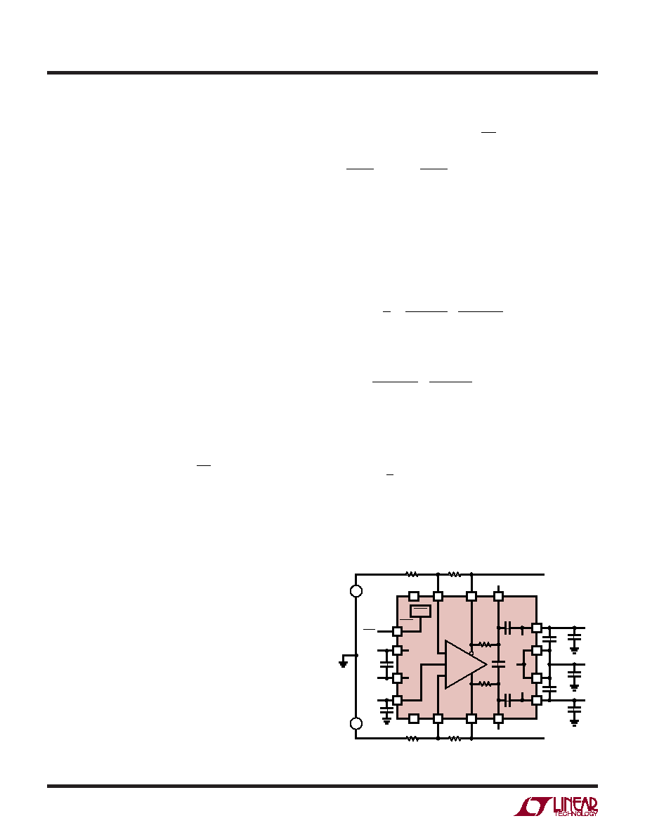
Effects of Resistor Pair Mismatch
Figure 3 shows a circuit diagram with takes into consid-
eration that real world resistors will not perfectly match.
Assuming innite open loop gain, the differential output
relationship is given by the equation:
VV
V
R
V
OUTDIFF
OUT
F
I
INDIFF
AVG
I
=≈
+
Δ
+
–
–
β
N
NCM
AVG
OCM
V
–
Δβ
β
where:
RF is the average of RF1, and RF2, and RI is the average
of RI1, and RI2.
βAVG is dened as the average feedback factor (or gain)
from the outputs to their respective inputs:
βAVG
I
IF
I
IF
R
RR
R
RR
=
+
1
2
1
11
2
22
Δβ is dened as the difference in feedback factors:
Δ=
++
β
R
RR
R
RR
I
IF
I
IF
2
22
1
11
–
VINCM is dened as the average of the two input voltages
VINP, and VINM (also called the source-referred input com-
mon mode voltage):
VV
V
INCM
INP
INM
=+
()
1
2
and VINDIFF is dened as the difference of the input
voltages:
VINDIFF = VINP – VINM
Figure 3. Real World Application With Feedback Resistor
Pair Mismatch
V–
V+
0.1
μF
0.1
μF
0.1
μF
0.1
μF
0.1
μF
–
+
1
SHDN
5
6
–IN
7
+OUT
8
+OUTF
16
15
+IN
NC
14
–OUT
13
–OUTF
V–OUTF
RF2
V+OUTF
V–OUT
V+OUT
2
V+
3
V–
V+
V–
V+
V–
4
VOCM
VSHDN
VVOCM
VOCM
12
V–
11
V+
10
V+
9
V–
64031 F03
LTC6403-1
SHDN
0.1
μF
0.01
μF
RF1
RI2
RI1
+
–
VINP
–
+
VINM
V–IN
V+IN
相关PDF资料 |
PDF描述 |
|---|---|
| AD9744ARURL7 | IC DAC 14BIT 210MSPS 28-TSSOP |
| LT6109HMS-2#PBF | IC AMP CURRENT SENSE 10-MSOP |
| LTC6403CUD-1#PBF | IC AMP/DRIVER LN LP 16-QFN |
| 74AHC1G14GV,125 | IC SCHMITT-TRG INV GATE SOT-753 |
| 74HC1G00GV,125 | IC 2-INPUT NAND GATE SC-74A |
相关代理商/技术参数 |
参数描述 |
|---|---|
| LTC6403IUD-1-TRPBF | 制造商:LINER 制造商全称:Linear Technology 功能描述:200MHz, Low Noise, Low Power Fully Differential Input/Output Amplifi er/Driver |
| LTC6404 | 制造商:LINER 制造商全称:Linear Technology 功能描述:600MHz, Low Noise, High Precision Fully Differential Input/Output Amplifi er/Driver |
| LTC6404-1 | 制造商:LINER 制造商全称:Linear Technology 功能描述:16-Bit, 20Msps ADC |
| LTC6404-2 | 制造商:LINER 制造商全称:Linear Technology 功能描述:2.7GHz, 5V, Low Noise,Rail-to-Rail Input Differential Amplifier/Driver |
| LTC6404-4 | 制造商:LINER 制造商全称:Linear Technology 功能描述:2.7GHz, 5V, Low Noise,Rail-to-Rail Input Differential Amplifier/Driver |
发布紧急采购,3分钟左右您将得到回复。