参数资料
| 型号: | LTC660CS8#TRPBF |
| 厂商: | Linear Technology |
| 文件页数: | 7/12页 |
| 文件大小: | 0K |
| 描述: | IC REG DBL INV ADJ 0.1A 8SOIC |
| 标准包装: | 2,500 |
| 类型: | 倍增器,反相 |
| 输出类型: | 可调式 |
| 输出数: | 1 |
| 输出电压: | -1.5 V ~ -5.5 V,5 V ~ 11 V |
| 输入电压: | 1.5 V ~ 5.5 V,2.5 V ~ 5.5 V |
| 频率 - 开关: | 10kHz,80kHz |
| 电流 - 输出: | 100mA |
| 同步整流器: | 无 |
| 工作温度: | 0°C ~ 70°C |
| 安装类型: | 表面贴装 |
| 封装/外壳: | 8-SOIC(0.154",3.90mm 宽) |
| 包装: | 带卷 (TR) |
| 供应商设备封装: | 8-SOIC |
�� �
�
�LTC660�
�APPLICATIO� N� S� I� N� FOR� M� ATIO� N�
�V� +�
�REQUIRED� FOR� TTL� LOGIC�
�V� +�
�7.0I�
�I�
�NC�
�1�
�8�
�100k�
�BOOST�
�(1)�
�C1�
�+�
�2�
�3�
�4�
�LTC660�
�7�
�6�
�5�
�–(V� +� )�
�OSC� INPUT�
�C2�
�OSC�
�SCHMITT�
�LV�
�(6)�
�7.0I�
�I�
�(7)�
�~� 18pF�
�TRIGGER�
�LTC660� ?� F05�
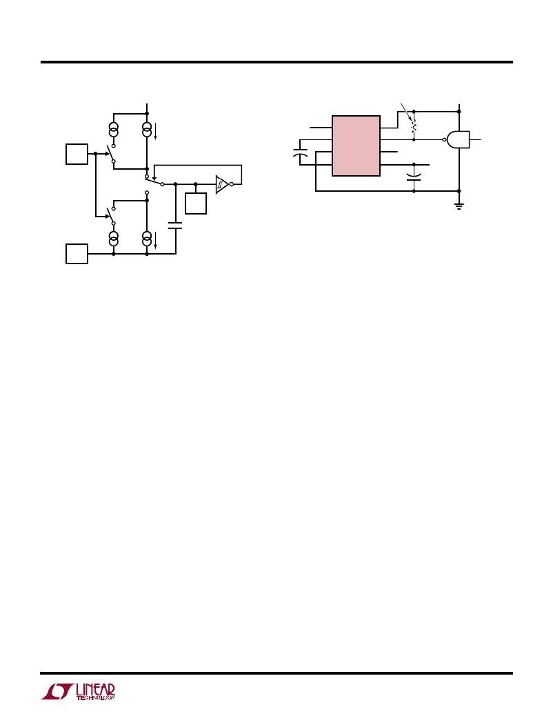
�Figure� 6.� External� Clocking�
�Capacitor� Selection�
�LTC660� ?� F06�
�Figure� 5.� Oscillator�
�By� connecting� the� BOOST� pin� (Pin� 1)� to� V� +� ,� the� charge� and�
�discharge� current� is� increased� and,� hence,� the� frequency�
�is� increased� by� approximately� four� and� a� half� times.�
�Increasing� the� frequency� will� decrease� output� impedance�
�and� ripple� for� high� load� currents.�
�Loading� Pin� 7� with� more� capacitance� will� lower� the� fre-�
�quency.� Using� the� BOOST� (Pin� 1)� in� conjunction� with�
�external� capacitance� on� Pin� 7� allows� user� selection� of� the�
�frequency� over� a� wide� range.�
�Driving� the� LTC660� from� an� external� frequency� source� can�
�be� easily� achieved� by� driving� Pin� 7� and� leaving� the� BOOST�
�pin� open,� as� shown� in� Figure� 6.� The� output� current� from�
�Pin� 7� is� small,� typically� 1.1� μ� A� to� 8� μ� A,� so� a� logic� gate� is�
�capable� of� driving� this� current.� (A� CMOS� logic� gate� can� be�
�used� to� drive� the� OSC� pin.)� For� 5V� applications,� a� TTL� logic�
�gate� can� be� used� by� simply� adding� an� external� pull-up�
�resistor� (see� Figure� 6).�
�While� the� exact� values� of� C1� and� C2� are� noncritical,� good�
�quality,� low� ESR� capacitors� are� necessary� to� minimize�
�voltage� losses� at� high� currents.� For� C1� the� effect� of� the� ESR�
�of� the� capacitor� will� be� multiplied� by� four,� due� to� the� fact�
�the� switch� currents� are� approximately� two� times� higher�
�than� the� output� current� and� losses� will� occur� on� both� the�
�charge� and� discharge� cycle.� This� means� using� a� capacitor�
�with� 1� ?� of� ESR� for� C1� will� have� the� same� effect� as�
�increasing� the� output� impedance� of� the� LTC660� by� 4� ?� .�
�This� represents� a� significant� increase� in� the� voltage� losses.�
�For� C2� the� effect� of� ESR� is� less� dramatic.� A� C2� with� 1� ?� of�
�ESR� will� increase� the� output� impedance� by� 1� ?� .� The� size�
�of� C2� and� the� load� current� will� determine� the� output�
�voltage� ripple.� It� is� alternately� charged� and� discharged� at�
�a� current� approximately� equal� to� the� output� current.� This�
�will� cause� a� step� function� to� occur� in� the� output� voltage� at�
�the� switch� transitions.� For� example,� for� a� switching� fre-�
�quency� of� 5kHz� (one-half� the� nominal� 10kHz� oscillator�
�frequency)� and� C2� =� 150� μ� F� with� an� ESR� of� 0.2� ?� ,� ripple� is�
�approximately� 90mV� with� a� 100mA� load� current.�
�7�
�相关PDF资料 |
PDF描述 |
|---|---|
| LTC6801HG#TRPBF | IC BATTERY MON MULTICELL 36SSOP |
| LTC6802IG-1#TRPBF | IC MONITOR BATT STACK MC 44-SSOP |
| LTC6803HG-1#TRPBF | IC MONITOR BATT STACK 44-SSOP |
| LTC692CN8 | IC MPU SUPERVISORY CIRCUIT 8-DIP |
| LTC6943HGN#TRPBF | IC BUILDNG BLK SWCAP DUAL 16SSOP |
相关代理商/技术参数 |
参数描述 |
|---|---|
| LTC6652 | 制造商:LINER 制造商全称:Linear Technology 功能描述:Precision Low Drift Low Noise Buffered Reference |
| LTC6652_1208 | 制造商:LINER 制造商全称:Linear Technology 功能描述:Precision Low Drift Low Noise Buffered Reference |
| LTC6652AHLS8-2.5#PBF | 功能描述:IC VREF SERIES PREC 2.5V RoHS:是 类别:集成电路 (IC) >> PMIC - 电压基准 系列:- 标准包装:2,000 系列:- 基准类型:旁路,可调节,精度 输出电压:1.24 V ~ 16 V 容差:±0.5% 温度系数:- 输入电压:1.24 V ~ 16 V 通道数:1 电流 - 阴极:100µA 电流 - 静态:- 电流 - 输出:20mA 工作温度:-40°C ~ 85°C 安装类型:通孔 封装/外壳:TO-226-3、TO-92-3(TO-226AA)成形引线 供应商设备封装:TO-92-3 包装:带卷 (TR) |
| LTC6652AHMS8-1.25 | 制造商:LINER 制造商全称:Linear Technology 功能描述:Precision Low Drift Low Noise Buffered Reference |
| LTC6652AHMS8-1.25#PBF | 功能描述:IC VREF SERIES PREC 1.25V 8-MSOP RoHS:是 类别:集成电路 (IC) >> PMIC - 电压基准 系列:- 标准包装:3,000 系列:- 基准类型:旁路,精度 输出电压:3V 容差:±0.5% 温度系数:100ppm/°C 输入电压:- 通道数:1 电流 - 阴极:82µA 电流 - 静态:- 电流 - 输出:15mA 工作温度:-40°C ~ 85°C 安装类型:表面贴装 封装/外壳:6-TSSOP(5 引线),SC-88A,SOT-353 供应商设备封装:SC-70-5 包装:带卷 (TR) 其它名称:296-20888-2 |
发布紧急采购,3分钟左右您将得到回复。