- 您现在的位置:买卖IC网 > PDF目录3492 > LTC6912HGN-2#TRPBF (Linear Technology)IC PGA DIGITAL R-R DUAL 16SSOP PDF资料下载
参数资料
| 型号: | LTC6912HGN-2#TRPBF |
| 厂商: | Linear Technology |
| 文件页数: | 13/24页 |
| 文件大小: | 0K |
| 描述: | IC PGA DIGITAL R-R DUAL 16SSOP |
| 标准包装: | 2,500 |
| 放大器类型: | 可编程增益 |
| 电路数: | 2 |
| 输出类型: | 满摆幅 |
| 转换速率: | 26 V/µs |
| 增益带宽积: | 30MHz |
| 电压 - 输入偏移: | 125µV |
| 电流 - 电源: | 2.25mA |
| 电流 - 输出 / 通道: | 35mA |
| 电压 - 电源,单路/双路(±): | 2.7 V ~ 10.5 V,±2.7 V ~ 5.25 V |
| 工作温度: | -40°C ~ 125°C |
| 安装类型: | 表面贴装 |
| 封装/外壳: | 16-SSOP(0.154",3.90mm 宽) |
| 供应商设备封装: | 16-SSOP |
| 包装: | 带卷 (TR) |
LTC6912
20
6912fa
APPLICATIO S I FOR ATIO
WU
UU
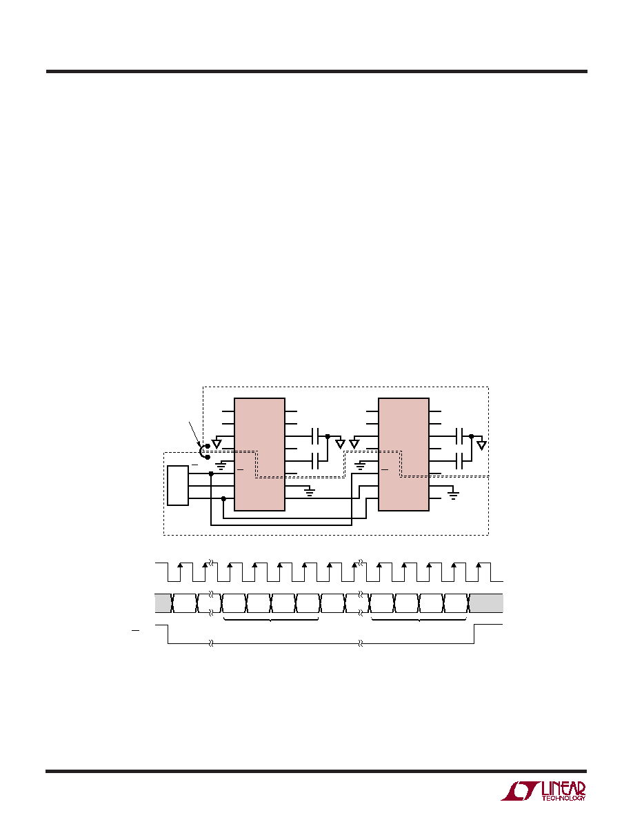
Figure 6. Two LTC6912s (Four PGAs) in Daisy Chain Configuration
1
2
3
4
5
6
7
8
16
15
14
13
12
11
10
9
LTC6912-X
0.1
F
0.1
F
V+
V–
DIGITAL GROUND PLANE
ANALOG GROUND PLANE
6912 F06
DGND
DOUT
1
2
3
4
5
6
7
8
16
15
14
13
12
11
10
9
LTC6912-X
0.1
F
0.1
F
V+
V–
DGND
DOUT
CS/LD
DATA
CLK
P
SINGLE-POINT
SYSTEM GND
D15
D11
D10
D9
D8
D7
D3
D2
D1
D0
CLK
DIN
CS/LD
SHDN
CS/LD
DIN
SHDN
CS/LD
DIN
configuration. It is recommended the serial interface sig-
nals should remain idle in between data transfers in order
to minimize digital noise coupling into the analog path.
Power On Reset
On the initial application of power, the power on reset
state of both amplifiers is low power software shutdown
(state = 8) (see Tables 1 and 2). In this state, both analog
amplifiers are disabled and have their inputs and outputs
opened. This will facilitate the application of using the
device as a 2:1 analog MUX, in that the amplifier’s outputs
may be wired-OR together and the LTC6912 can alter-
nately select between A and B channels. Care must be
taken if the outputs are wired-OR’d to ensure the software
shutdown state (state = 8) is always programmed in one
of the two channels.
Timing Constraints
Settling time in the CMOS gain-control logic is typically
several nanoseconds and is faster than the analog signal
path. When the amplifier gain changes, the limiting timing
is analog. As with any programmable-gain amplifier, each
gain change causes an output transient as the amplifier’s
output moves, with finite speed, toward a differently
scaled version of the input signal. The LTC6912-X analog
path settles with a characteristic time constant or time
scale,
τ, that is roughly the standard value for a first order
band limited response:
τ = 0.35/f–3dB
See the –3dB BW vs Gain Setting graph in the Typical
Performance Characteristics section.
相关PDF资料 |
PDF描述 |
|---|---|
| 5-103817-8 | 30 MODII HDR 3RST UNSHRD .100 |
| RW3R0DB100RJET | RES POWER 100 OHM 3W 5% SMD |
| CLT-108-01-L-D | CONN RCPT 16POS DUAL 2MM T/H |
| RW3R0DB15R0JET | RES POWER 15 OHM 3W 5% SMD |
| CLT-138-02-G-D | CONN RCPT 76POS DUAL 2MM SMD |
相关代理商/技术参数 |
参数描述 |
|---|---|
| LTC6912IDE-1 | 制造商:LINER 制造商全称:Linear Technology 功能描述:Dual Programmable Gain Amplifiers with Serial Digital Interface |
| LTC6912IDE-1#PBF | 功能描述:IC PGA DIGITAL R-R DUAL 12-DFN RoHS:是 类别:集成电路 (IC) >> Linear - Amplifiers - Instrumentation 系列:- 标准包装:100 系列:- 放大器类型:通用 电路数:1 输出类型:- 转换速率:0.2 V/µs 增益带宽积:- -3db带宽:- 电流 - 输入偏压:100pA 电压 - 输入偏移:30µV 电流 - 电源:380µA 电流 - 输出 / 通道:- 电压 - 电源,单路/双路(±):±2 V ~ 18 V 工作温度:0°C ~ 70°C 安装类型:表面贴装 封装/外壳:8-SOIC(0.154",3.90mm 宽) 供应商设备封装:8-SO 包装:管件 |
| LTC6912IDE-1#TRPBF | 功能描述:IC PGA DIGITAL R-R DUAL 12-DFN RoHS:否 类别:集成电路 (IC) >> Linear - Amplifiers - Instrumentation 系列:- 标准包装:2,500 系列:- 放大器类型:通用 电路数:1 输出类型:满摆幅 转换速率:0.11 V/µs 增益带宽积:350kHz -3db带宽:- 电流 - 输入偏压:4nA 电压 - 输入偏移:20µV 电流 - 电源:260µA 电流 - 输出 / 通道:20mA 电压 - 电源,单路/双路(±):2.7 V ~ 36 V,±1.35 V ~ 18 V 工作温度:-40°C ~ 85°C 安装类型:表面贴装 封装/外壳:8-SOIC(0.154",3.90mm 宽) 供应商设备封装:8-SO 包装:带卷 (TR) |
| LTC6912IDE-2 | 制造商:LINER 制造商全称:Linear Technology 功能描述:Dual Programmable Gain Amplifiers with Serial Digital Interface |
| LTC6912IDE-2#PBF | 功能描述:IC PGA DIGITAL R-R DUAL 12-DFN RoHS:是 类别:集成电路 (IC) >> Linear - Amplifiers - Instrumentation 系列:- 标准包装:100 系列:- 放大器类型:通用 电路数:1 输出类型:- 转换速率:0.2 V/µs 增益带宽积:- -3db带宽:- 电流 - 输入偏压:100pA 电压 - 输入偏移:30µV 电流 - 电源:380µA 电流 - 输出 / 通道:- 电压 - 电源,单路/双路(±):±2 V ~ 18 V 工作温度:0°C ~ 70°C 安装类型:表面贴装 封装/外壳:8-SOIC(0.154",3.90mm 宽) 供应商设备封装:8-SO 包装:管件 |
发布紧急采购,3分钟左右您将得到回复。