- 您现在的位置:买卖IC网 > PDF目录3492 > LTC6912HGN-2#TRPBF (Linear Technology)IC PGA DIGITAL R-R DUAL 16SSOP PDF资料下载
参数资料
| 型号: | LTC6912HGN-2#TRPBF |
| 厂商: | Linear Technology |
| 文件页数: | 9/24页 |
| 文件大小: | 0K |
| 描述: | IC PGA DIGITAL R-R DUAL 16SSOP |
| 标准包装: | 2,500 |
| 放大器类型: | 可编程增益 |
| 电路数: | 2 |
| 输出类型: | 满摆幅 |
| 转换速率: | 26 V/µs |
| 增益带宽积: | 30MHz |
| 电压 - 输入偏移: | 125µV |
| 电流 - 电源: | 2.25mA |
| 电流 - 输出 / 通道: | 35mA |
| 电压 - 电源,单路/双路(±): | 2.7 V ~ 10.5 V,±2.7 V ~ 5.25 V |
| 工作温度: | -40°C ~ 125°C |
| 安装类型: | 表面贴装 |
| 封装/外壳: | 16-SSOP(0.154",3.90mm 宽) |
| 供应商设备封装: | 16-SSOP |
| 包装: | 带卷 (TR) |
LTC6912
17
6912fa
AGND: Analog Ground. The AGND pin is at the midpoint of
an internal resistive voltage divider, developing a potential
halfway between the V+ and V– pins. In normal operation,
the AGND pin has an equivalent input resistance of nomi-
nally 50k (Figure 1). In order to reduce the quiescent
supply current in hardware shutdown (SHDN pin pulled to
V+, GN-16 only), the equivalent series resistance of this
pin significantly increases (to a value on the order of
800k
with 5V supplies, but is highly supply voltage,
temperature, and process dependent). AGND is the
noninverting input to both the internal channel A and
channel B amplifiers. This makes AGND the ground refer-
ence voltage for the INA, INB, OUTA, and OUTB pins.
Recommended analog ground plane connection depends
on how power is applied to the LTC6912-X (See Figures 2,
3, and 4). Single power supply applications typically use
V– for the system signal ground. The analog ground plane
in single-supply applications should therefore tie to V–,
and the AGND pin should be bypassed to this ground plane
by a high quality capacitor of at least 0.1
F (Figure 2). The
AGND pin provides an internal analog reference voltage at
half the V+ supply voltage. Dual supply applications with
symmetrical supplies (such as
±5V) have a natural system
ground plane potential of zero volts, in which the AGND pin
can be directly tied to, making the zero volt ground plane
the input and output reference voltage for the LTC6912-X
(Figure 3). Finally, if dual asymmetrical power supplies are
used, the supply ground is still the natural ground plane
voltage. To maximize signal swing capability with an
asymmetrical supply, however, it is often desirable to refer
the LTC6912-X’s analog input and output to a voltage
equidistant from the two supply rails V+ and V–. The AGND
pin will provide such a potential when open-circuited and
bypassed with a capacitor (Figure 4). In noise sensitive
applications where AGND does not tie directly to a ground
plane, as in Figures 2 and 4, it is important to AC-bypass
the AGND pin. Otherwise channel to channel isolation is
degraded, and wideband noise will enter the signal path
from the thermal noise of the internal voltage divider
resistors which present a Thévenin equivalent resistance
of approximately 50k
. This noise can reduce SNR by at
least 15dB at high gain settings. An external capacitor
from AGND to the ground plane, whose impedance is well
below 50k
at frequencies of interest, will filter and
suppress this noise. A 0.1
F high quality capacitor is
effective for frequencies down to 1kHz. Larger capacitors
will extend this suppression to lower frequencies. This
issue does not arise in dual supply applications because
the AGND pin ties directly to ground. In applications
requiring an analog ground reference other than half the
total supply voltage, the user can override the built-in
analog ground reference by tying the AGND pin to a
reference voltage with the AGND voltage range specified in
the Electrical Characteristics Table. The AGND pin will load
the external reference with approximately 50k
returned
to the half-supply potential. AGND should still be capaci-
tively bypassed to a ground plane as noted above. Do not
connect the AGND pin to the V– pin.
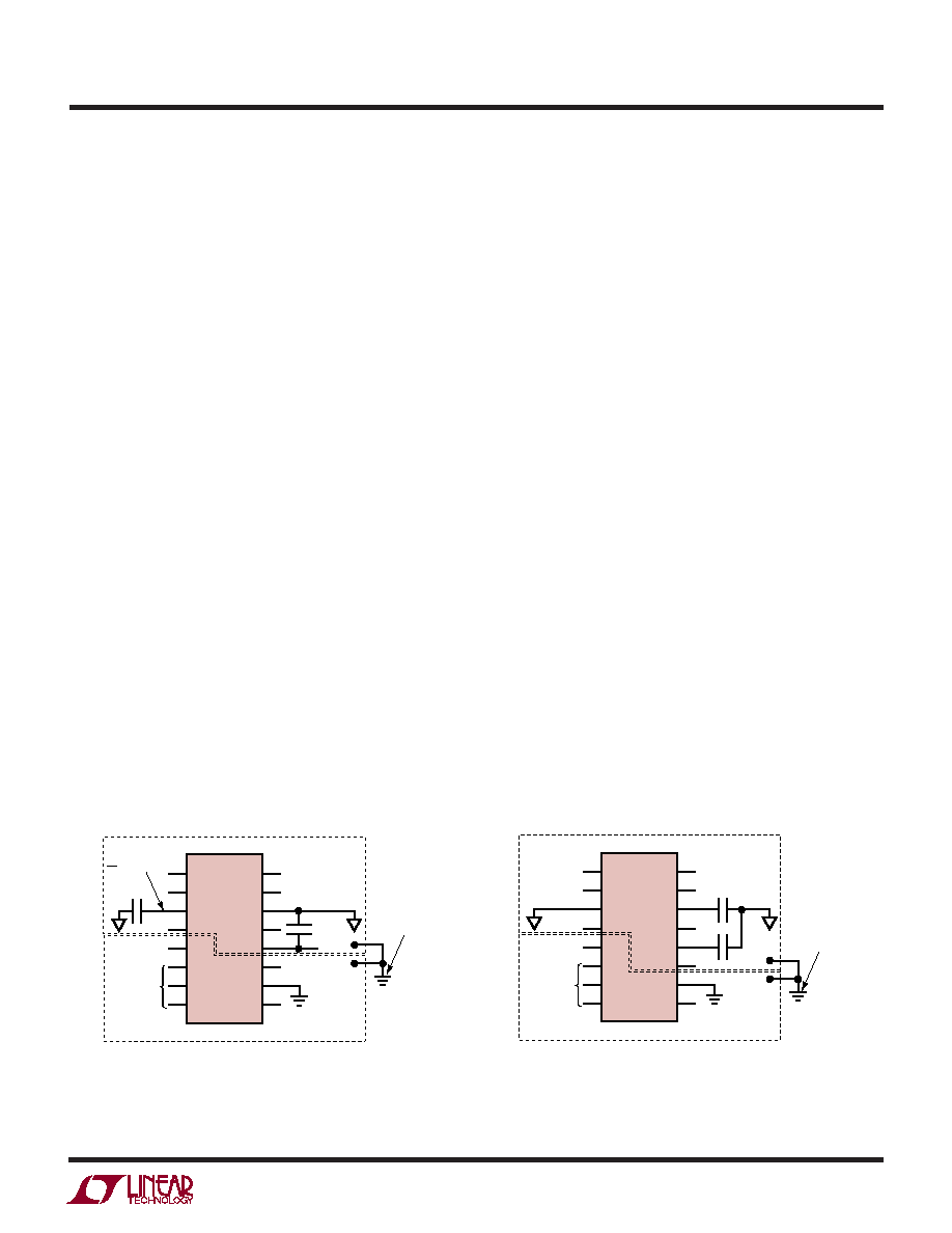
Figure 2. Single Supply Ground Plane Connection
1
2
3
4
5
6
7
8
16
15
14
13
12
11
10
9
LTC6912-X
SERIAL
INTERFACE
0.1
F
V+
DIGITAL GROUND PLANE
ANALOG GROUND PLANE
SINGLE-POINT
SYSTEM GND
≥0.1F
V+
2
REFERENCE
6912 F02
UU
U
PI FU CTIO S
Figure 3. Symmetrical Dual Supply Ground Plane Connection
1
2
3
4
5
6
7
8
16
15
14
13
12
11
10
9
LTC6912-X
SERIAL
INTERFACE
0.1
F
0.1
F
V+
V–
DIGITAL GROUND PLANE
ANALOG GROUND PLANE
6912 F03
SINGLE-POINT
SYSTEM GND
相关PDF资料 |
PDF描述 |
|---|---|
| 5-103817-8 | 30 MODII HDR 3RST UNSHRD .100 |
| RW3R0DB100RJET | RES POWER 100 OHM 3W 5% SMD |
| CLT-108-01-L-D | CONN RCPT 16POS DUAL 2MM T/H |
| RW3R0DB15R0JET | RES POWER 15 OHM 3W 5% SMD |
| CLT-138-02-G-D | CONN RCPT 76POS DUAL 2MM SMD |
相关代理商/技术参数 |
参数描述 |
|---|---|
| LTC6912IDE-1 | 制造商:LINER 制造商全称:Linear Technology 功能描述:Dual Programmable Gain Amplifiers with Serial Digital Interface |
| LTC6912IDE-1#PBF | 功能描述:IC PGA DIGITAL R-R DUAL 12-DFN RoHS:是 类别:集成电路 (IC) >> Linear - Amplifiers - Instrumentation 系列:- 标准包装:100 系列:- 放大器类型:通用 电路数:1 输出类型:- 转换速率:0.2 V/µs 增益带宽积:- -3db带宽:- 电流 - 输入偏压:100pA 电压 - 输入偏移:30µV 电流 - 电源:380µA 电流 - 输出 / 通道:- 电压 - 电源,单路/双路(±):±2 V ~ 18 V 工作温度:0°C ~ 70°C 安装类型:表面贴装 封装/外壳:8-SOIC(0.154",3.90mm 宽) 供应商设备封装:8-SO 包装:管件 |
| LTC6912IDE-1#TRPBF | 功能描述:IC PGA DIGITAL R-R DUAL 12-DFN RoHS:否 类别:集成电路 (IC) >> Linear - Amplifiers - Instrumentation 系列:- 标准包装:2,500 系列:- 放大器类型:通用 电路数:1 输出类型:满摆幅 转换速率:0.11 V/µs 增益带宽积:350kHz -3db带宽:- 电流 - 输入偏压:4nA 电压 - 输入偏移:20µV 电流 - 电源:260µA 电流 - 输出 / 通道:20mA 电压 - 电源,单路/双路(±):2.7 V ~ 36 V,±1.35 V ~ 18 V 工作温度:-40°C ~ 85°C 安装类型:表面贴装 封装/外壳:8-SOIC(0.154",3.90mm 宽) 供应商设备封装:8-SO 包装:带卷 (TR) |
| LTC6912IDE-2 | 制造商:LINER 制造商全称:Linear Technology 功能描述:Dual Programmable Gain Amplifiers with Serial Digital Interface |
| LTC6912IDE-2#PBF | 功能描述:IC PGA DIGITAL R-R DUAL 12-DFN RoHS:是 类别:集成电路 (IC) >> Linear - Amplifiers - Instrumentation 系列:- 标准包装:100 系列:- 放大器类型:通用 电路数:1 输出类型:- 转换速率:0.2 V/µs 增益带宽积:- -3db带宽:- 电流 - 输入偏压:100pA 电压 - 输入偏移:30µV 电流 - 电源:380µA 电流 - 输出 / 通道:- 电压 - 电源,单路/双路(±):±2 V ~ 18 V 工作温度:0°C ~ 70°C 安装类型:表面贴装 封装/外壳:8-SOIC(0.154",3.90mm 宽) 供应商设备封装:8-SO 包装:管件 |
发布紧急采购,3分钟左右您将得到回复。